Latest News Special Report Research Result Column Profiles Laboratory Descriptions
![]() Congratulations! GIPO Professor
Chi-Kuang Sun is engaged as NTU’s “Distinguished Professor” beginning from
August 1st, 2008 to July 31st, 2011.
Congratulations! GIPO Professor
Chi-Kuang Sun is engaged as NTU’s “Distinguished Professor” beginning from
August 1st, 2008 to July 31st, 2011.
![]() Congratulations! GIPO Professor Jian-Jang Huang receives the
2008 Ta-You Wu Memorial Award from the National Science Council.
Congratulations! GIPO Professor Jian-Jang Huang receives the
2008 Ta-You Wu Memorial Award from the National Science Council.
![]() GIPO
Academic
Visiting
Highlights
GIPO
Academic
Visiting
Highlights
|
August GIPO Lecture Highlights |
|
|
Time: August 11th, 2008, 10:30 a.m. ~ 11:45 a.m. Speaker: Prof. Ray T. Chen (Nanophotonics and Optical Interconnects Lab., Department of Electrical and Computer Engineering, The University of Texas, Austin) Topic: Silicon- and Polymer-based Nanophotonic Devices for Optical Communications Prof. Ray T. Chen visited GIPO on August 11th (Monday), 2008 and lectured in room 142, the EE Building II. The lecture, “Silicon- and Polymer-based Nanophotonic Devices for Optical Communications” was attended with enthusiasm by GIPO professors and students, and everyone learned much. |
|
|
Time: August 25th, 2008, 3:00 p.m. Speaker: Prof. Sailing He (Joint Research Center of Photonics of the Royal Institute of Technology (Sweden) and Zhejiang University (China)) Topic: Improving the Performances and Functionalities of Photonics Devices with Subwavelength-structures and Nanoparticles Prof. Sailing He visited GIPO on August 25th (Monday), 2008, and lectured in lecture hall 105, the EE Building II. The lecture “Improving the Performances and Functionalities of Photonics Devices with Subwavelength-structures and Nanoparticles” was attended with enthusiasm by GIPO professors and students. |
|


![]() Words from Kuang-Chung Liu, President of the GIPO Student
Association, 2008 academic year:
Words from Kuang-Chung Liu, President of the GIPO Student
Association, 2008 academic year:
![]()
|
It is a great honor to be the president of the GIPO Student Association for 2008 academic year. First of all, I'd like to thank all the students of GIPO for giving me this opportunity to serve. I'd also like to thank classmates Hung-Li Chiang, Kun-Mao Pan and Shih-Hua Hsiao for assisting me in handling association affairs and laboratory duties , so that I may concentrate on the task at hand. Since my admission in September 2007, I've spent a year in this large GIPO family. There are many factors which lead me to take on the position of president, the following being most important. During that year at GIPO, I attended classes, carried out experiments, played soccer, socialized, and spent nearly all my time with my classmates. When I was happy, they shared my happiness; when I felt discouraged in the face of setbacks, my friends were at my side, providing advice and encouragement. I experienced nothing but warmth and kindness from professors and classmates, bringing me to the realization that I am a part of this big family. I will do my best to serve GIPO and bring to you all the happiness that I've found here. |
|
|
During the past year, I often heard classmates mention that GIPO held too few activities compared with other EECS institutes, which is rather a pity. Therefore, in the coming year, the GIPO Student Association’s main objective will be to hold a variety of exciting social activities to promote friendship among laboratories. Activities will include social lunches or dinners, sporting competitions, arts and culture events, and much more. Please get ready to participate in the fun! Also, we are looking forward to building communication between students, administrators and professors enabling students to speak out about GIPO affairs and be heard. Compared with some of my senior classmates, I'm quite new to GIPO. Nevertheless, in my term, I will devote all my heartfelt passion and sincerity to the GIPO Student Association. Please feel free to offer your comments, suggestions, and aid so that we can provide everyone with the best possible service. |
|

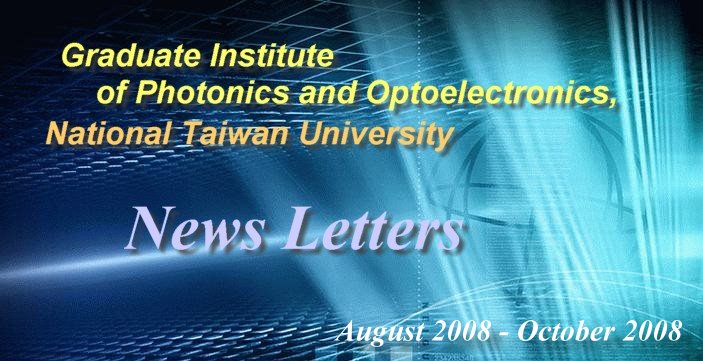
![]() GIPO Student Association 2008 Badminton Tournament Highlights
GIPO Student Association 2008 Badminton Tournament Highlights
![]()
September 8th, 2008
3F, NTU Sports Center
Kuang-Chung Liu, President of the GIPO Student Association
This year's GIPO badminton tournament was held on the afternoon of September 8th. The contestants were comprised of 48 students in 8 teams. Team 4 won the championship; teams 2, 3, 6 and 7 were tied at second, all having attained the same final score. Although several students couldn't make it in time to take part in the tournament, they still came to play during breaks. Encouraging everyone to exercise more is precisely the intent behind organizing this tournament. This year’s tournament has come to a successful ending. In practicing badminton skills, and bonding with fellow classmates, we hope that everyone can forget about winning or losing and bring their passion and enthusiasm to the next GIPO sporting event.
 |
 |
|
Contestants warm up |
Jump smash |
 |
 |
| Someone’s stomach gets in the picture | Battling courageously in spite of wearing dress shoes |
 |
 |
| Lowerclassmen girls also participating in the badminton tournament | The winning team |
 |
 |
| This year’s best contestant | Resting courtside |
![]() Research Result Column for the Program of
“Aiming for Top University”
Research Result Column for the Program of
“Aiming for Top University”
Optical Characterization of CO2-Laser-ablated Si rich SiOx
Professor Gong-Ru Lin
Graduate Institute of Photonics and Optoelectronics, National Taiwan University
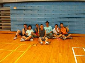
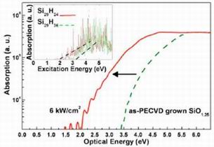
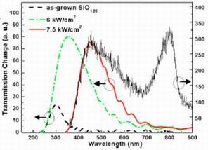
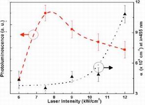
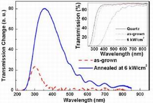
Anomalous absorption and the corresponding change in the optical band gap of a CO2-laser-ablated Si-rich (SiOx) film are studied. The optical band gap energy of as-grown nonstoichiometric SiOx is slightly reduced by increasing Si–Si bonds as compared to quartz. After rapid thermal annealing using a CO2 laser, the dehydrogenation of SiOx film further increases the Si–Si bonding states and redshifts the optical band gap by 1 eV (see Figure 1a and 1b). Laser ablation is initiated at a laser intensity of >7.5 kW/cm2 (see Figure 2), leaving numerous luminescent centers that are related to neutral oxygen vacancy defects, increasing the absorption coefficient and related optical band gap energy, and reducing the refractive index in partially annealed SiOx (see Figure 3a and 3b).
In summary, the anomalous absorption spectra and corresponding changes in optical band gap energy, band edge absorption, and structurally damaged related luminescent centers of the CO2-laser-ablated PECVD-grown SiO1.25 film were characterized using UV-VIS-NIR transmission/ reflection and PL spectroscopies. After PECVD deposition, a slight redshift in the transmission and the lower optical band gap energy of as-grown SiO1.25 in comparison with those of quartz substrate are due to the increase in the Si–Si bonding state in SiO1.25 near the valence and conduction band edges. Since the as-grown SiO1.25 film contains a high concentration of hydrogen, dehydrogenation not only reduces the thickness of the PECVD-grown SiO1.25 film but also enhances the number of Si–Si bonding states under CO2 laser RTA below the ablation threshold (6 kW/cm2), hence contributing to a redshift of the optical band gap from 3.32 to 2.43 eV. As the CO2 laser RTA intensity increases to >6 kW/cm2, the optical band gap energy of the PECVD-grown SiO1.25 increases oppositely from 2.43 to 2.76 eV due to the ablation-induced damage to the surface and the generated NOV defects. The absorption coefficient of the SiO1.25 film at a wavelength of 455 nm is increased by a factor of 3 as the CO2 laser intensity is increased from 7.5 to 12 kW/cm2. During ablation, the incompletely annealed SiO1.25 with numerous oxygendependent defects also suffers from a slight decrease in the refractive indices from 1.87 to 1.79 when Plaser increases from 7.5 to 12 kW/cm2.
|
|
 |
|
FIG. 1a. Transmission change of as-grown SiO1.25 and CO2 laser annealed SiO1.25 at Plaser=6 kW/cm2. (Inset: Transmission spectra of pure quartz) |
FIG. 1b. Absorption spectra of as-grown SiO1.25 and CO2 laser annealed SiO1.25 at Plaser=6 kW/cm2. (Inset: The calculated absorption spectra of Si29H24 and Si29H36) |
 | |
|
FIG. 2. Optical band gap of CO2 laser annealed SiO1.25 as a function of laser intensity. (Inset: Tauc plot, (ahn) 1/2 as a function of photon energy (hn) for as-grown SiO1.25 sample and CO2 laser RTA SiO1.25 samples at Plaser from 6 to 12 kW/cm2) | |
 |
 |
|
FIG. 3a. PL spectrum of PECVD-grown SiO1.25 annealed at CO2 Plaser of 7.5 kW/cm2 and transmission change of as-grown SiO1.25 and CO2 laser annealed SiO1.25 at Plaser of 6 and 7.5 kW/cm2. |
FIG. 3b. Refractive index and absorption coefficient of CO2 laser RTA SiO1.25 as a function of laser intensity. |
![]()
![]()
Patterned microlens array for efficiency improvement of small-pixelated organic light-emitting devices
Research groups of Prof. Hoang-Yan Lin and Prof. Jiun-Haw Lee
Graduate Institute of Photonics and Optoelectronics, National Taiwan University
(e-mail) hylin@cc.ee.ntu.edu.tw
We experimentally and theoretically investigated the optical characteristics of organic light-emitting devices (OLEDs), having different pixel sizes and attached with patterned microlens array films. For a regular microlens array (Fig. 1(b)), though it can extract the waveguiding light and increase luminous current efficiency for a large-pixelated OLED, we observed that it decreased the luminance to an even lower level than that of the planar OLED as its pixel size was close to the microlens dimension (Fig. 2). Although a microlens can effectively outcouple the light rays originally at incident angles larger than the critical angle, it also can impede the outcoupling for the light rays originally at incident angles smaller than the critical angle. Enhancement or reduction of the light extraction depends on the relative positions of the light emitting point and the microlens. Therefore, we proposed a center-hollowed microlens array (Fig. 1(c)), of which the microlenses directly upon the pixel are removed, and proved that it can increase the luminous current efficiency and luminous power efficiency of a small-pixelated OLED. As can be seen from Fig. 3, by attaching this patterned microlens array, 87% of luminance enhancement in the normal direction was observed for a 0.1´0.1 mm2 OLED pixel. On the other hand, a regular microlens array resulted in 4% decrease under the same condition.
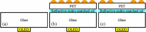 |
| Fig. 1. The OLEDs attached (a) without, and with (b) a regular and (c) a center-hollowed microlens array. |
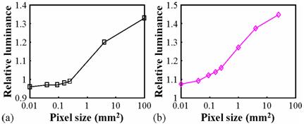 |
| Fig. 2. The relationships between the relative luminance at normal direction and the pixel size of the OLEDs attached with regular microlens arrays: (a) experimental and (b) simulated results. |
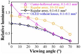 |
| Fig. 3. The angular-dependent luminance of the OLED attached with a regular microlens array or with a center-hollowed array. |
| *This paper was published in OPTICS EXPRESS, Vol. 16, No. 15, pp. 11044-11051, 21 July 2008. |
![]()
![]()
Electrical and Optical Characteristics of OLED with Bipolar Emitting Layer
Research group of Prof. Jiun-Haw Lee
Graduate Institute of Photonics and Optoelectronics, National Taiwan University
One of the root causes which limits the operation lifetime of organic light-emitting device (OLED) is the charged carriers piled-up at the interface of transporting layer and emitting layer (EML). By introducing the bipolar EML, the recombination zone in an OLED becomes wider which effectively elongated the operation lifetime. We have demonstrated the performance improvement and studied the electrical and optical characteristics of OLEDs with bipolar EML quantitatively and qualitatively.
We used high-electron-mobility ETL material, bis(10-hydroxybenzo[h] qinolinato)beryllium (Bebq2), mixed with a-naphthylphenylbiphenyldiamine (NPB) as the bipolar EML. We have demonstrated an OLED with a luminance of 27600 cd/m2 at only 5 V, and a lifetime four times longer than that of a conventional device. Since the recombination zone was wider, the maximum luminance in a bipolar OLED can be as high as 288000 cd/m2 with the current density over 7 A/cm2, which may be suitable for flashlight applications. Not only the performance improvement, we also discussed the carrier transport characteristics in a bipolar EML from current-voltage characteristics and the recombination process from the electro-luminescence measurement. We found an optimized mixing ratio which was NPB:Bebq2=1:1 with highest current density due to the electron-hole balance in this bipolar EML. The spectral shift was due to the recombination shift and the solid-state solvation effect.
Besides, we used two different methods to quantitatively investigate the recombination zone in the MH-EML consisting of NPB and tris-(8-hydroxyquinoline) aluminum (Alq3). The first method was by using rigorous electrical and optical models to simulate the carrier distribution, recombination distribution, and EL spectra in the MH-OLED. By fitting the J-V curves and the spectra with different mixing ratios, the mobility values can be extracted. Electron (hole) mobility decreased (increased) monotonically with increasing the NPB ratio. However, the driving voltage increased then decreased due to the competition between the hole-current enhancement and the electron-current decline. For the second method, we used a thin 4-(dicyanomethylene)-2-tert-butyl-6-1,1,7,7-(tetramethyljulolidyl-9-enyl)-4H-pyran (DCJTB) layer with the thickness of 1.2 nm and the volume concentration of 2% as a probe to determine the recombination zone. Besides, we also found that when the probe position overlapped the maximum recombination position, a voltage reduction of 1.97 V was observed. It can be well explained by the enhancement of the recombination current from the continuity equation. This result suggested that the driving voltage of an OLED with the bipolar EML can be reduced by inserting a dopant in a suitable region. A white OLED was fabricated with selectively doping a yellow dopant in the blue EML which exhibits high efficiency and low driving voltage.
![]()
![]()
Ferroelectric nitride-oxide nanowire MOSFET and phase change memory
Professor Lung-Han Peng's group
Graduate Institute of Photonics and Optoelectronics, National Taiwan University
(e-mail) peng@cc.ee.ntu.edu.tw
A. Nitride-oxide nanowire MOSFET
We demonstrated a selective growth of high crystallinity
![]() GaN
nanowire (NW) with high channel mobility of 1050cm2/V-s
on SiO2/p-Si with optimized VLS growth
parameters. Then, we successfully fabricated top-gate
GaN nanowires FETs by the photolithography process. High
crystalline nanowire approach favors the device scaling
of low dimensional n-MOSFET and logic circuitry. Our
data from a 60nm diameter GaN top-gated nanowires n-MOSFET
exhibit an encouraging gm value of 24mS
measured at the device saturation regime. This number is
one order of magnitude larger than its competitive III-V
compound nanowire transistor. At a moderate 1V gate
bias, the device exhibits a current driving density of
60mA,
VT to -1.5V, ON/OFF current ratio over 103,
and subthreshold swing to 150mV/dec.
GaN
nanowire (NW) with high channel mobility of 1050cm2/V-s
on SiO2/p-Si with optimized VLS growth
parameters. Then, we successfully fabricated top-gate
GaN nanowires FETs by the photolithography process. High
crystalline nanowire approach favors the device scaling
of low dimensional n-MOSFET and logic circuitry. Our
data from a 60nm diameter GaN top-gated nanowires n-MOSFET
exhibit an encouraging gm value of 24mS
measured at the device saturation regime. This number is
one order of magnitude larger than its competitive III-V
compound nanowire transistor. At a moderate 1V gate
bias, the device exhibits a current driving density of
60mA,
VT to -1.5V, ON/OFF current ratio over 103,
and subthreshold swing to 150mV/dec.
B. Nitride-oxide phase change memory
We report a new type of phase-change materials based upon the compound of In-Ga-O. It is found to exhibit two-order of magnitude resistivity change between the high-resistive amorphous phase and the low-resistive cubic phase at a phase-change temperature ~250°C. When the In-Ga-O is incorporated into a nonvolatile phase change memory (PCM) device with a double-heater (DH) structure, it exhibits an on/off resistance ratio of 1000 and cycling over 300 times which are superior to those observed on a single-heater (SH) PCM device. These results, together with a low bias point of 70mA at 6.5 volt and 1.5mA at 3.5 volt, respectively, for set/ reset operation of the DH-PCM device to the crystalline/amorphous state, suggest that In-Ga-O is a promising material candidate for low power application of PCM devices.
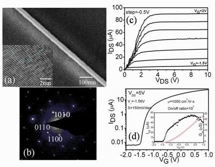 |
| Figure 1 (a) SEM micrograph of a 60nm GaN NW grown on SiO2/p-Si. Inset:High–resolution TEM showing lattice image and spacing of 0.272 nm of GaN NW. (b) electron diffraction patterns revealing six-fold rotation symmetry of GaN and high crystallinity diffraction signals. (c) DC characteristics of top-gate NW-MOSFET. (d) Transfer characteristics of a 60nm-dia. GaN NW-MOSFET. |
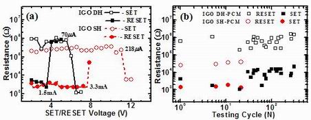 |
| Figure 2 (a) SET / RESET programming R-V curve of 30nm-thick IGO PCM devices with CA~40.1mm2, with the 80ns SET electric pulse at 6.5V/70mA and the 20ns RESET pulse at 3.5V/1.5mA. (b) Cycling-endurance test for the IGO DH and SH PCM devices. The DH-PCM device shows a better performance of cycle-endurance (~300 times) than SH-PCM. The IGO film thickness is 30nm. |
![]()
![]()
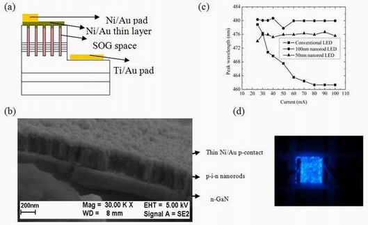
GaN nanorod light emitting diode arrays with a nearly constant electroluminescent peak wavelength
Prof. JianJang Huang
Graduate Institute of Photonics and Optoelectronics, National Taiwan University
We present a practical process to fabricate InGaN/GaN MQW structure using silica nanoparticle nature lithography. The EL peak wavelength occurs in the range of 478~480nm and 474~476nm for 100nm and 50nm nanorod LEDs, respectively, with injection currents between 25mA and 100mA. As compared with the significant blue shift in planar structures (from 478nm to 461nm), the piezoelectric field is suppressed on nanorod LEDs since the strain in InGaN layers is relaxed. We also carried out Raman measurement to study the strain relaxation of the nanostructures. The Raman shift of nanorods is lower than that of planar MQW structure. It indicates strain relaxed nanorod light emitting devices are achieved with a nearly constant peak wavelength.
|
|
| Figure (a) Device profiles of nanorod LEDs. SOG (in pink) is coated between rods as a space and sidewall passivation layer. (b) An SEM image of 100nm-diameter. (c) Comparison of peak wavelengths of conventional, 50nm and 100nm nanorod LEDs. (d) Light emission of a 100nm nanorod LED with an injection current 20mA. |
![]()
![]()
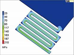
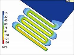
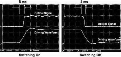
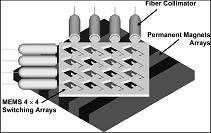
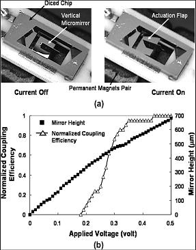
Low-Actuation-Voltage MEMS for 2-D Optical Switches
Hsin-Ta Hsieh and Prof. Guo-Dung John Su
Graduate Institute of Photonics and Optoelectronics, National Taiwan University
A novel MEMS fabrication process was developed to integrate vertical stress-free micromirrors and electromagnetic actuators without an extra assembly process. The size of the TMAH etched micromirror is 20 μm × 500 μm × 1200 μm, which is large enough to ensure low insertion loss for 2-D optical-switching applications. The surface roughness of the micromirror is measured to be as low as 20 nm by the white light interferometer, which typically results in 0.2-dB optical loss. The center-aligned vertical mirror showed an excellent TDL of 0.05 dB. An appropriate magnetic circuit design reduces the actuation voltage to 0.5 V with a power consumption of about 3.5 mW. A reasonable fast-switching time of 5 ms can be achieved by eliminating the resonant-frequency components of the MEMS switch through edited waveforms. Long-term cycling and mechanical reliability tests proved that the proposed MEMS optical switch can pass the rigorous requirement of optical communications. The PDL and WDL are both less than 0.1 dB.
|
|
 |
 |
|
|
(a) Operated device and (b) applied voltage versus normalized coupling efficiency and moving heights. |
Stress analysis for corner design effect. |
 |
 |
|
Switching time of a 2-D MEMS switch. |
Schematic drawing of a 4 × 4 MEMS optical switch with periodical magnet ribbons. |
![]()
![]()
Finite-Difference Modeling of Dielectric Waveguides with Slanted Facets
Y.-P Chiou, Y.-C. Chiang, C.-H. Lai, C.-H. Du, and H.-C. Chang
Graduate Institute of Photonics and Optoelectronics, National Taiwan University
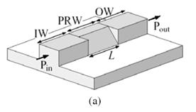
Abstract -- With the help of an improved finite-difference (FD) formulation, we investigate the propagation characteristics of a slant-faceted polarization converter. The formulation is full-vectorial and it takes into consideration discontinuities of fields and their derivatives across the abrupt interfaces. Hence, the limitations in conventional FD formulation are alleviated. Field behaviors across the slanted facet are incorporated in the formulation and hence the staircase approximation in conventional FD formulation is removed to get better modeling of the full-vectorial properties.
One limitation of conventional finite-difference method is that grids in the computation are normally parallel to the axes in the discretization of field components. Staircase approximation is often required when the fields are cross a slanted interface between two different materials. The convergence is slow due to the staircase approximation as compared to other methods without staircase approximation, e.g. finite-element method. In addition, the full-vectorial properties may not be accurately modeled under such approximation. To get rid of such limitation, our improved finite-difference method is adopted.
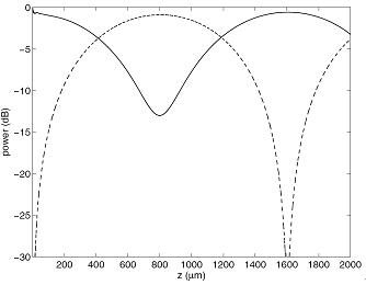
The investigated structure is shown in Fig.1. An x-polarized field is launched from a standard input waveguide (IW). This incident field excites both the first and second hybrid modes of nearly equal modal amplitudes. As these two hybrid modes propagate along the polarization rotating waveguide (PRW), they would become out of phase at the half-beat length and their combined modal fields produce mainly a y-polarized field in the following output waveguide (OW). The polarization rotating waveguideis based on a rib waveguide with one side wall slanted at an angle around 45 degrees.
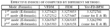
In the structure, both hybrid modes have comparable field components in x- and y- directions, and their polarizations are no longer mainly in the x- or y- direction but in the direction parallel or perpendicular to the slanted wall. As shown in Fig.2, the field is periodically converted between x- and y- polarizations. To verify our simulation, finite-element method (FEM) and Yee-mesh-based finite-difference beam propagation method (Yee-FD-BPM) are adopted as shown in Table I. Both electrical and magnetic fields are used at the same time in the formulation of Yee-FD-BPM. Different methods show very good agreement. Furthermore, we also use conventional finite-difference scheme with staircase approximation and index-average approximation to calculate the same problem. We find that the hybrid modes can not be correctly obtained either by our codes or by commercial software. The fundamental modes may become x- or y-dominant modes, not as expected. To sum up, our improved finite-difference scheme can easily handle structures with facets that are not parallel to x- or y-axis, which alleviates the limitation in conventional finite-difference method.
 |
 |
| Fig.1 (a) Polarization converter (b) Cross-section view. | |
 |
|
| Fig.2 Power in x- (solid line) and y- (dashed line) polarized fields along the propagation. | |
| Table I | |
 |
|
![]()
![]()
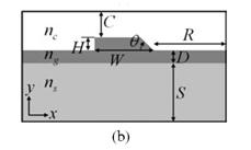
Design and Analysis of Compact Slot Waveguide Directional Coupler-Based Polarization Splitter on Silicon-on-Insulator
Professor Ding-wei Huang
Graduate Institute of Photonics and Optoelectronics, National Taiwan University
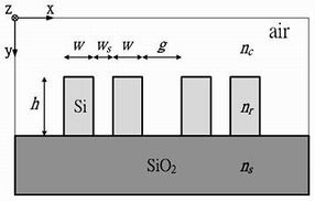
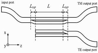
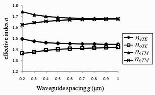
A slot waveguide directional coupler-based polarization splitter on SOI which exhibits excellent polarization splitting behavior for optical signals around 1.55 mm is designed and analyzed. In our design, the silicon photonic wire is covered by air (nc = 1) and patterned on the buried oxide layer (ns = 1.444) of the SOI wafer, where the low-refractive-index region (slot region) is sandwiched by high-refractive-index silicon (nr = 3.474) at 1.55 μm as shown in Fig.1. The schematic layout of the entire device is shown in Fig. 2. The width w and height h of each photonic wire at the slot region is chosen to be 0.21 μm and 0.25 μm; while the width of the slot ws is set to be 0.2 μm due to the limitation of the fabrication capability. The propagation of light in the directional coupler can be expressed in terms of even and odd modes with effective indices ne and no, which are functions of the waveguides spacing g as shown in Fig. 3. By carefully choosing the spacing g (g = 0.48 μm) between the two waveguides, the coupling length of TE mode LTE can be twice that of TM mode LTM, i.e. LTE /LTM = 2. Meanwhile the length of the coupling region of the device is chosen to be L = 2LTM = LTE, thus the two modes can be successfully separated into 2 different output ports. By using FDTD technique, the electric field intensities of the TE- and TM-polarized modes propagating in the device can be calculated as shown in Fig. 4.
 |
 |
| Fig. 1 A cross-sectiional view of slot directional coupler-based polarization splitter. |
Fig. 2 Schematic layout of the entire device. |
 |
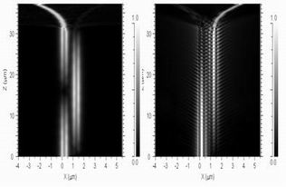 |
| Fig. 3 Effective indexes of even modes ne and odd modes no induced in TE polarization (neTE, noTE) and TM polarization (neTM, noTM) of a coupler as a function of waveguide spacing g. | Fig. 4 Polarization splitting behavior in the device. The left-hand side is the result of TM mode and the right-hand side is the result of TE mode. |
Please send comments to GIPO_5@cc.ee.ntu.edu.tw.
Copyright
Graduate Institute of Photonics and Optoelectronics, National Taiwan University