Latest News Special Report Research Result Column Profiles Laboratory Descriptions
![]() Congratulations! GIPO Professor Jr Hau He receives “The
Exploration Research Award 2008 of Pan Wen Yuan Foundation”.
Congratulations! GIPO Professor Jr Hau He receives “The
Exploration Research Award 2008 of Pan Wen Yuan Foundation”.
![]() Congratulations! GIPO Professor Chi-Kuang Sun receives “The
6th Y. Z. Hsu Scientific Paper Award” (Nano Science & Technology Category).
Congratulations! GIPO Professor Chi-Kuang Sun receives “The
6th Y. Z. Hsu Scientific Paper Award” (Nano Science & Technology Category).
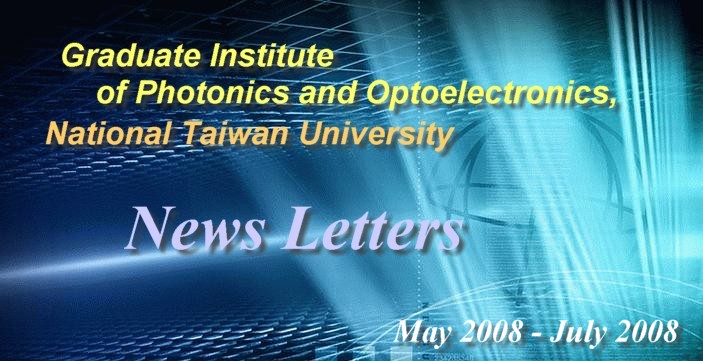
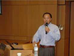
![]() Dr. James C. Wyant, Vice President of the Optical Society of
America, and Dean of the College of Optical Sciences, University of Arizona,
visited GIPO on June 11th, 2008.
Dr. James C. Wyant, Vice President of the Optical Society of
America, and Dean of the College of Optical Sciences, University of Arizona,
visited GIPO on June 11th, 2008.
|
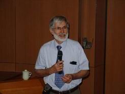
Dr. James C. Wyant, Vice President of the Optical Society of America, and Dean of the College of Optical Sciences, University of Arizona visited GIPO on the morning of June 11th. Accompanied by Professor Cheng-Chung Lee, Professor Wyant visited Chairman Sheng-Lung Huang, Dean Pei, and several professors of GIPO. Professor Wyant also toured laboratories of GIPO, and everyone took this valuable opportunity to share their research experiences and achievements. |
 |
|
Dr. James C. Wyant (middle) with Professor Cheng-Chung Lee (right), and GIPO Chairman Sheng-Lung Huang (left). |
![]() GIPO
Academic
Visiting
Highlights
GIPO
Academic
Visiting
Highlights
|
April “Photonics Forum” Lecture Highlights |
|
|
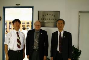
Time: April 11th, 2008, 4:30 pm Speaker: Mr. Lin, Cheng-Hui (Chairman, Dan-Lu Calligraphy Society) Topic: A Rambling Talk about Calligraphy Mr. Lin, Cheng-Hui visited GIPO on April 11th, 2008 (Friday), and lectured in the Auditorium of Barry Lam Hall. His lecture, “A Rambling Talk about Calligraphy” was attended with enthusiasm by GIPO professors and students. Everyone learned much. |
|
|
May “Photonics Forum” Lecture Highlights |
|
|
Time: May 23rd, 2008, 4:30~6:30 pm Speaker: Professor Zhu, Shining (Member of Chinese Academy of Sciences, Chairman of the Department of Physics, Nanjing University) Topic: Engineering Ferroelectric Domain for Nonlinear Photonics Professor Zhu, Shining visited GIPO on May 23rd, 2008 (Friday) and lectured in the Auditorium of Barry Lam Hall. His topic, “Engineering Ferroelectric Domain for Nonlinear Photonics” inspired enthusiastic participation and discussion among participating GIPO professors and students, and everyone learned much. |
|
|
Time: May 30th, 2008, 4:30~6:30 pm Speaker: Prof. Cun-Zheng Ning (Center for Nanophotonics-Arizona Institute of NanoElectronics, Center of Solid State Electronics Research (CSSER) and Department of Electrical Engineering, Arizona State University) Topic: Surface Plasmonic and Nanowire Lasers : What is the Ultimate Size Limit? Professor Cun-Zheng Ning visited GIPO on May 30th, 2008, and lectured in the Auditorium of Barry Lam Hall. His topic, “Surface Plasmonic and Nanowire Lasers : What is the Ultimate Size Limit?” inspired enthusiastic participation and discussion among participating GIPO professors and students, and everyone learned much. We look forward to Professor Cun-Zheng Ning’s next visit to GIPO. |
|
|
June “Photonics Forum” Lecture Highlights |
|
|
Time: June 13th, 2008, 4:30~6:30 pm Speaker: Dr. Jean-Pierre Monchalin (Group Leader, Optical Diagnostics of Materials, Modelling and Diagnostics, Industrial Materials Institute, National Research Council of Canada, Canada) Topic: Optical Coherence Tomography and Ultrasound Modulated Optical Imaging at the Industrial Materials Institute of the National Research Council of Canada Dr. Jean-Pierre Monchalin visited GIPO on June 13th, 2008 (Friday) and lectured in the Auditorium of Barry Lam Hall. His lecture, “Optical Coherence Tomography and Ultrasound Modulated Optical Imaging at the Industrial Materials Institute of the National Research Council of Canada” was attended with enthusiasm, and everyone learned much. |
|
![]() 2008 Academic
Exchange with Nanjing
University
Ph.D. Students
2008 Academic
Exchange with Nanjing
University
Ph.D. Students
![]()
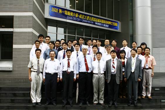
【The 1st Ph.D. Student Forum between National Taiwan University and Nanjing University on Photonic Microstructures and Laser Technologies, 2008】
May 19th-20th, 2008
National Taiwan University
Highlights Compilation: GIPO Ph.D. candidate Sen-Ming Hsu (team leader of the GIPO student representatives)
First, I would like to thank Graduate Institute of Photonics and Optoelectronics (GIPO) for offering the opportunity of a meaningful academic exchange activity with the Department of Physics, Nanjing University. I would also like to acknowledge my advisor, Professor Hung-Chun Chang, whose recommendation made me one of the representatives of GIPO in this event. This was an invaluable experience and excellent learning chance.
The 1st Ph.D. Student Forum between National Taiwan University and Nanjing University on Photonic Microstructures and Laser Technologies 2008 was held in Taiwan. Chairman of the Department of Physics, Nanjing University, Professor Shining Zhu, along with three faculty members and nine students, journeyed to GIPO in the hopes of sharing their phenomenal academic achievements with us. In order to well-organize the activity and show them our hospitality, after all the student members of GIPO delegation were decided, the first preparatory meeting was immediately held in February. It’s my honor to be elected as the student group leader of NTU, who would be responsible for communication and coordination with the head student representative of Nanjing University, Mr. Bin Liu. I was delighted to collaborate with Mr. Bin Liu, whose assistance made both the preparatory work and the activity course very successful.
The exchange conference took place on May 19th and 20th. Topics reported were diverse and profound, including nano-photonics, photonic bandgap devices, nonlinear photonic devices, multiferroic materials, wide bandgap semiconductors, and OLED devices, etc. Each student was delegated to give a 25-minute oral presentation, introducing his/her laboratory and personal research accomplishments. During the conference, many non-delegate students volunteered to assist the grand occasion and various GIPO professors attended and gave their precious advice and encouragements to the participants. Unlike previous exchange conferences with other universities, in which the participants communicated in English, all the speakers made their speeches in Chinese, expecting the knowledge sharing and communication between both parties to be more straightforward. Many speakers and participants joined discussions with great enthusiasm after presentations, and continued to do so during the breaks, a phenomenon showed that both parties were intrigued in the research topics of each other’s. In the two-day academic conference, we indeed realized the outstanding research achievements of the Department of Physics, Nanjing University. Each delegate from Nanjing University has achieved high-level research accomplishments. It was delightful to learn and brainstorm with such great company.
When we were planning the conference agenda, aside from the interaction between the student delegates, we also invited Dr. Ping Xu and Dr. Liang Sun of the Department of Physics, Nanjing University, to address us on the second day of the conference. This suggestion was promptly accepted by both of them so we were able to listen to their wonderful speeches introducing their spectacular research achievements and thus gained much knowledge. Special thanks to Dr. Ping Xu and Dr. Liang Sun for their kindness for giving wonderful speeches.
Besides the conference itself, visits to related laboratories, research centers, and companies were scheduled during this exchange activity for the delegates of the Department of Physics, Nanjing University. In addition to the laboratories belonging to GIPO professors, other laboratories/centers such as Nano-Electro-Mechanical-System (NEMS) Research Center and Center for Condensed Matter Sciences (CCMS) in NTU were also included on the schedule. We also arranged tours to National Synchrotron Radiation Research Center (NSRRC) and AU Optronics Corp. (AUO) in Hsinchu. We deeply appreciated the kindness of all the laboratories, research centers, and companies mentioned above for providing the delegates of the Department of Physics, Nanjing University a good chance to learn from their experience.
As a participant in this activity, I not only got to know many great new friends from Nanjing University, but also was thrilled to meet many more GIPO Ph.D. students. Every member counted in this conference and I could not thank you more for your contributions.
Last but not least, I would like to thank Chairman of GIPO, Sheng-Lung Huang, and Vice Chairman of GIPO, Gong-Ru Lin, for their generosity to guide us on planning this event. From the preliminary work to the attentive efforts during the activity, both professors had shared their experience with us and their sharing spared us a lot of time and work. Also, without GIPO staff, Ms. Hsiao-Wen Lin, none of this could have been possible. I hope that, such an activity shall be a yearly event in the future, so that more of GIPO students can benefit from it and put what they learn to real practice.
 |
|
The professors and students of both participating parties. |
![]()
Highlights compilation: GIPO Ph.D. candidate Yen-Cheng Lu (deputy team leader of the GIPO student representatives)
I was honored to attend the GIPO and Nanjing University academic exchange activity. After several months of preparation and a few temporary setbacks, the professors and students from Nanjing University finally arrived in Taiwan on May 18th, and the workshop began on the 19th as planned. This year’s exchange included three parts: academic workshops, laboratory tours, and cultural tours. The itinerary was as follows:
|
2008.05.18(Sunday) |
Arrival of Nanjing University representatives in Taiwan |
|
2008.05.19(Monday) |
Academic Exchange Workshop |
|
2008.05.20(Tuesday) |
Academic Exchange Workshop |
|
2008.05.21(Wednesday) |
Laboratory Tours (GIPO, Center for Condensed Matter Sciences, and Gallery of NTU History |
|
2008.05.22(Thursday) |
Cultural Tours (Maokong Gondola, Chiang Kai-shek Memorial Hall (Liberty Square), Taipei 101, and Shilin Night Market) |
|
2008.05.23(Friday) |
Laboratory Tours (National Synchrotron Radiation Research Center and AU Optronics Corp.) |
|
2008.05.24(Saturday) |
Cultural Tours (National Palace Museum and Danshuei) |
|
2008.05.25(Sunday) |
Nanjing University representatives left Taiwan |
With the support of Chairman Sheng-Lung Huang, Vice Chairman Gong-Ru Lin, Ms. Hsiao-wen Lin, and the hard work of all participating members, the workshop was a great success. For NJU and NTU students, this was a journey that touched their minds and hearts, and was filled with native culture and scientific exchange. The participating students were as follows: Sen-Ming Hsu (team leader), Cha-Hsin Chao, Hsing-Chieh Cheng, Chang-Ting Lin, Jeng-Jie Huang, Shan-Chuang Pei, Cheng-Pin Chen, Jeng-Wei Yu and me. Unfortunately, Kuang-Li Lee was unable to attend due to a family emergency. However, we deeply appreciate the wonderful posters and nametags that he designed for us during our preparations for this event. Lastly, thank you to Nan-Fu Chiu for stepping in and filling Kuang-Li’s place in the group.
Most of us were quite used to attending academic workshops, but few of us had actually had the experience of organizing one. When measured against international workshops usually involving hundreds of people, this particular workshop, involving twenty people, was a small-scale operation in comparison. However, through the experience of preparing for and participating in the workshop and the entire exchange, I’ve come to realize that it takes a lot more than I imagined to make such an event run smoothly and successfully. I’ve learned a lot from this experience. Many of my fellow students were extremely knowledgeable about Taipei, even Taiwan, and I felt slightly ashamed as I was only familiar with traveling between school and home. Chang-Ting is familiar with the geography of Hsinchu, and with Taiwanese industry. Shan-Chuang and Cheng-Pin know all about Taiwan’s famous scenic spots and fine food. Hsing-Chieh is an expert guide; listening to him introducing Taiwan to the Nanjing students left me in awe of his understanding. In fact, the laboratory and cultural tours took me to places that I hadn’t visited in a long time, or had never visited before, and I must thank the students who arranged these wonderful and exciting excursions. This event has added a whole new level to my understanding of life.
During the exchange with students from Mainland China, it was inevitable that the most sensitive topic of conversation would be Cross-Strait relations between China and Taiwan. I’m sure that everyone is curious as to how we all handled this situation. In fact, the students from Mainland China rarely brought up any topic related to this issue, whether it was during this year’s exchange with NJU students, or last year’s visit to Tsing Hua University in Beijing; of course, we did not mention the topic either. This must be what the popular saying “set aside conflict, create success together” means. We were all very cautious during our exchanges, afraid that we might generate the spark that could light the fire, so to speak, and create unpleasantness between the two parties. During one of my conversations with an NJU student, I asked him, “So, is this your first time out of the country?” His face showed shock, as though he didn’t know quite how to answer my question, and I quickly realized my mistake. Before he found an answer, I rephrased my question, “Is this your first time out of Mainland China?” upon which he answered yes with a smile. Aside from these instances, being around the students from Mainland China was very similar to being around my Taiwanese classmates. Everyone’s main topic of interest was still the differences between China and Taiwan. The school system in China requires three years for a master’s degree, and three years for a doctor’s degree. The Taiwanese school system on the other hand, normally requires two years for a master’s degree, and from three up to seven years for a doctorate, depending on one’s academic performance. Also, I was told that in China, a person with a master’s degree who found a good job could receive a starting salary of about $5000RMB. On the other hand, a person with a doctorate who remained at the university to become a lecturer (similar to our assistant professor level) would receive a starting salary of less than $4000RMB. This was one of the more surprising differences for me, as I know that in Taiwan, it is almost impossible for a person with a master’s degree to receive a higher starting salary than a person with a doctor’s degree.
Lastly, as Chang-Ting told our Nanjing University guests, we were participating in an exchange with them, and among ourselves at the same time. Before taking part in this event, many of our classmates were not familiar with each other, or did not know each other at all. This academic exchange gave everyone an opportunity to get together. In recent years, GIPO has held frequent exchange activities with universities outside of Taiwan. However, exchange within GIPO itself seems less frequent in comparison. Perhaps as we continue exchange with universities outside of Taiwan, we can also organize events within GIPO. This may create an even more positive atmosphere.
|
|
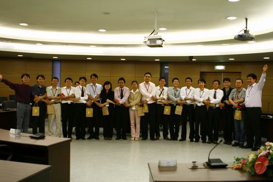
| Students who participated in the workshop exchanged gifts and were photographed together. |
![]() Research Result Column for the Program of
“Aiming for Top University”
Research Result Column for the Program of
“Aiming for Top University”
Silicon waveguide sidewall smoothing by KrF excimer laser reformation
Shih-Che Hung and Prof. Ching-Fuh Lin
Graduate Institute of Photonics and Optoelectronics, National Taiwan University
Silicon photonics has been an active research field of integrated optics, where low-cost, compact, and integrated optical components are dedicatedly pursued. Compact, small-core waveguides, however, suffers from excessive scattering loss due to the sidewall roughness, which prohibits building dense integrated optoelectronic circuits.
Many efforts are devoted to sidewall smoothing of Si waveguides to reduce the scattering loss, including hydrogen annealing, dry oxidation, wet chemical etching, and so on. However, methods using high temperature have a thermal budget constraint on the pre-built electronics. Oxidation methods have low capability of reducing large roughness. Developing a technique capable of optoelectronic integration and high capability of roughness reduction for compact, integrated, and high performance Si waveguides has been a challenging goal.
The principle of laser reformation for smooth Si waveguides is to melt the sidewall by a high energy laser pulse at an incident angle, as illustrated in Fig. 1. The molten Si of the sidewall reforms due to the surface tension and hence gives the name of this technique. In this technique, the quantity of energy absorbed by silicon from excimer laser highly depends on the incident angle of the laser beam due to transmission coefficient of this electromagnetic wave at interface. In order to selectively exposure sidewall rather than top surface and substrate, the incoming laser beam is designated to illuminate on the Si ridge at a greatly inclined angle. This configuration allows laser to mainly melt the sidewall at a suitable energy density.
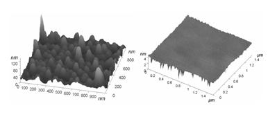
The as-etched Si surface has a RMS roughness of 14 nm, as shown in Fig. 2 (left). As shown in this figure, the highest protrusion on the as-etched surface even exceeds 100 nm. Laser illumination with an energy density of 1.4 J/cm2 is applied at normal incidence. By one shot of laser pulse, the RMS roughness of the laser-reformed surface reduces to 0.28 nm. By 5 shots of laser pulses, the RMS roughness reduces to 0.24 nm. The AFM photo of Si surface illuminated by 5 shots is shown in Fig. 2 (right). Such a high roughness reduction is due to surface tension which enables the surface area to be the minimum by nature.
AFM measurement shows the RMS roughness is reduced from 14 nm to 0.24 nm. Scattering loss of waveguides with such a small sidewall roughness is calculated to be 0.033 dB/cm. Compared to other processes like hydrogen annealing, dry oxidation and wet chemical etching, the laser reformation technique shows unique capabilities of flattening protrusions as high as 100 nm and of selective exposure. Good surface quality investigated from the MWPCD measurements also supports the laser-reformation method to fabricate optoelectronic devices.
|
|
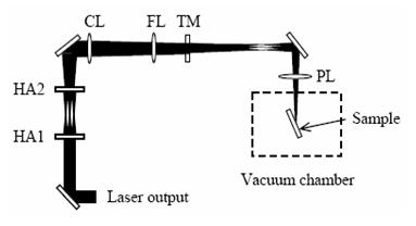
| Fig. 1. The homogenizer and projection lens setup of KrF excimer laser. |
 |
|
Fig. 2. AFM scans of the as-etched surface (left) and the surface after laser illumination by 5 shots of laser pulses with energy density of 1.4 J/cm2 (right). |
![]()
![]()
Cr4+:YAG double-clad crystal fiber laser
Chien-Chih Lai, Kuang-Yao Huang, Hann-Jong Tsai, Zhi-Wei Lin, Kuan-Dong Ji, and Sheng-Lung Huang
Graduate Institute of Photonics and Optoelectronics, National Taiwan University
(e-mail) slhuang@cc.ee.ntu.edu.tw
Cr4+:YAG has demonstrated very good performance in terms of laser and amplified spontaneous emission sources due to the interaction of its 3d2 electronic configuration with lattice vibration levels. In order to effectively confine the pumping light and emission, crystal fiber core with glass cladding is preferable since a significant reduction both in the scattering loss and the number of propagating modes can be achieved. Of particular importance, with the Cr4+:YAG as the core and silica as the cladding, it has been shown that the emission generated by the core can be easily guided due to the large fractional index change at the core/inner-cladding interface. Furthermore, numerous passive fiber elements, such as connectors, splitters, and isolators, permit the construction of laser resonators in all-fiber configuration. No external optical elements are required by direct dielectric coating onto the fiber ends. Low optical loss and gain-guided propagation are the superiorities for fiber lasers to achieve low-threshold lasing. Double-clad Cr4+:YAG crystal fiber (Cr4+:YAG DCF) grown by a co-drawing laser-heated pedestal growth method can offer continuous-wave (CW) pumped, low-threshold, and low-cost coherent sources operated at room-temperature for all-fiber communications systems. In this article, we report the lasing characteristics of Cr4+:YAG DCF with a record-lowest threshold among all Cr4+:YAG lasers.
To investigate the lasing behavior of the Cr4+:YAG DCF and efficiently remove the heat generated in the fiber, a 16.5-mm-long fiber was mounted into Cu-Al alloy and clamped to a copper heat sink. A CW Yb fiber laser at 1064 nm was initially focused by an 10X objective and then incident into a single-mode fiber (HI-1060, Thorlabs) followed by a thin-film based 1060/1550 coupler to monitor the lasing spectra by an OSA. The pump beam passes through a standard telecommunication fiber (SMF-28) and was butt-coupled to the core of the Cr4+:YAG DCF through a dichroic-coated front end face. The crystal fiber laser output and the pump beam were collimated by a 10-mm achromatic lens and further filtered by a long-wavelength-pass filter before been detected by a photo detector.
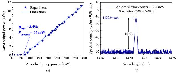
The measured and simulated laser output powers of the Cr4+:YAG DCF laser as a function of the absorbed pump power are shown in Fig. 1(a). The threshold power is 69 mW with an output coupler transmittance of 2.5%. The maximun laser output power (limited by the damage threshold of the 1060/1550 coupler) as high as 11.2 mW was achieved as the absorbed pump power was 385 mW. Figure 1(b) shows the lasing spectrum at ~ 1421 nm of the maximum absorbed pump power. The lasing spectrum measured with a resolution bandwidth of 0.08 nm at the maximum absorbed pump power, showing a side mode suppression ratio (SMSR) of 45 dB.
|
|
|
Fig. 1. Lasing characteristics of the room-temperature CW Cr4+:YAG DCF laser. (a) The laser output power of Cr4+:YAG DCF laser as a function of the absorbed pump powers. The threshold and slope efficiency are 69 mW and 3.4% with the output coupler transmittance of 2.5%, respectively. (b) Measured lasing spectra at ~ 1,421 nm under the maximum absorbed pump power, showing a 45-dB SMSR. |
|
Cr4+:YAG crystal fiber laser with double-clad structure has been successfully developed. The 69 mW threshold is the lowest and the 3.4% slope efficiency is the highest as compared with any bulk or fiber Cr4+:YAG lasers at room temperature. The performance of this Cr4+:YAG DCF laser can be further improved by optimizing the output coupler transmittance, crystal fiber length, and decreasing crystal fiber temperature by proper thermal management. Additionally, the Cu-Al alloy diffusion process allows for cladding-pump configuration with multimode diode lasers as pump sources to offer a high-brightness output. Furthermore no external optical elements are required by direct dielectric-coating onto the fiber ends. This leads to a compact, low material consumption, and low-cost crystal fiber lasers. The desirable features associated with numerous passive fiber elements, such as connectors, splitters, and isolators, permit the construction of all-fiber configuration. This laser is a promising candidate for demonstrating broadband tunability for future all-optical communication systems. |
![]()
![]()
SiGe Based Optoelectronics
T. -H. Cheng and C. W. Liu
Graduate Institute of Photonics and Optoelectronics, National Taiwan University
(e-mail) chee@cc.ee.ntu.edu.tw
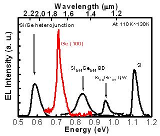
It is a long sought goal to integrate ultra-large scale integrated (ULSI) circuits with the electro-optics to possibly overcome the speed limitation of electrical interconnects and to add extra functionalities on Si chip. LEDs and detectors are essential devices to achieve this goal. The most common material systems used for the light-emitting technology are III-V-based systems. However, due to the compatibility with Si electronics, the Si-based light emitters are the holy grails for the full integration of electrical and optical devices. Besides the 1.1μm infrared emission from Si band edge, the addition of Ge into Si can tune the optical characteristic to longer wavelength infrared emission from ~1.1μm to ~2.2μm wavelength (Fig. 1). The wavelengths of ~1.3μm, ~1.5μm, and ~2.2μm infrared have been achieved by Si0.8Ge0.2 Quantum well, Si0.45Ge0.55 quantum dot, Si/Si0.2Ge0.8 type-II heterojunction MIS LED, respectively. Moreover, due to the high carrier mobility, strong photon absorption, and possible integration with Si, the Ge based optoelectronic device also attracts great interest for scientific research and practical applications, recently. We develop successfully a Ge MIS tunneling diodes to serve both as a light emitter (~1.8μm) and a photodetector at a suitable bias.
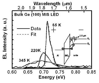
Figure 2 shows the EL spectra from an Al/SiO2/Ge MIS tunneling diode under continuous-wave operation at room temperature. The simulated line shapes from the electron-hole-plasma recombination model have a good agreement with the experimental data. The extracted band gaps using the electron hole plasma model are 40 meV lower than the Ge band gap obtained from Varshni’s equation from 65 to 345 K. This energy reduction is due to the longitudinal acoustic (LA) and longitudinal optic (LO) phonon replica in the radiative recombination, the band gap renormalization, and a significant amount of heat locally at the high injection current density. The inset of Fig. 2 depicts the schematic band diagram of the MIS tunneling diode for EL operation. At the positive gate voltage, an accumulation layer of majority electrons is formed at the Ge/SiO2 interface. The tunneling holes from the Al electrode recombine with electrons accumulated at the Ge/SiO2 interface and result in the radiative EL. Interface roughness, phonons, and the spread in k-space due to localized electrons can provide the extra momentum during the electron-hole-radiative recombination to emit the photons.
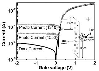
When the MIS tunneling diode is biased at the inversion region, it can serve as a photodetector. The typical dark and photo currents of a bulk Ge (100) MIS photodetector under different wavelength exposures are shown in Fig. 3. The Ge MIS photodetector has a responsivity of 0.180 and 0.053 A/W at the wavelengths of 1310 and 1550 nm, respectively. The main reasons for the smaller responsivity in the MIS structure are the interface states at the insulator/semiconductor interface and the larger light reflectance of Al electrode. The inset of Fig. 3 shows the band diagram of the Ge MIS photodetector at inversion bias. The inversion bias can cause the deep depletion region to collect the photo-generated carriers. The minority carriers are generated in the deep depletion region, tunnel from the active absorption layer to the Al gate electrode via the trap-assisted tunneling of the LPD oxide, and form the photocurrent.
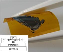
Data communication between the Ge MIS LED and the Ge MIS photodetector is also demonstrated up to 15 Mbit/sec. The speed limitation is mainly due to the function generator in our system and can be enhanced with the high-speed modulator or detector. Other photodetectors such as GOG (Ge-on-Glass), GOI (Ge-on-Insulator), and GOP (Ge-on-Polyimide) are also developed to reach the goal of low cost, high speed, and extra functionality by wafer bonding and smart-cut technique. Figure 4 shows the photograph of flexible GOP structure. The thickness of the transferred Ge layer is about 1.6 μm, and the surface roughness of the GOP structure is ~ 11 nm after the smart-cut process. Al with a ring area was evaporated on Ge. Since the Al ohmic contact has a large area (>0.1 cm2) and the barrier height between Al and Ge is small (0.1 eV), the effect of contact resistance is small. The low-temperature (50℃) liquid phase deposited (LPD) oxide and Pt gate were used as the gate stack inside the Al ring.
As time goes by, the solar cell plays a more and more important role to solve the energy crisis problem. In order to enhance the efficiency of solar cell, the simulation of optimized grid space, nano-texture structure, and external strain are added on the solar cell. The optical methods such as photoluminescence (PL) and electroluminescence (EL) are used to analysis the characteristics of solar cell. Minority carrier lifetime and diffusion length can be measured by temporal response of the electroluminescence and laser beam induced current (LBIC) to analysis the solar cell characteristics.
|
|
 |
|
FIG. 1 The emission spectra of SiGe based LEDs ( bulk Si, bulk Ge, SiGe QD, SiGe QW, and Si/SiGe heterojunction). It covers the wavelength from 1.1 μm to 2.2 μm. |
FIG. 2. The measured electroluminescence spectra of a bulk Ge MIS LED at different temperatures. The inset shows the schematic band diagram at the accumulation positive bias for the Ge MIS LED. |
|
|
|
|
|
|
FIG. 3. The dark and photo I-V characteristics of a Ge _100_ MIS photodetector under 1310 and 1550 nm lightwave exposure. The inset shows the schematic band diagram at the inversion (negative) bias for the Ge MIS photodetector. |
Fig. 4 The photograph of flexible Ge-on-polyimide structure after bending. The inset shows the device structure. |
Please send comments to GIPO_5@cc.ee.ntu.edu.tw.
Copyright
Graduate Institute of Photonics and Optoelectronics, National Taiwan University