|
November 2008 - February 2009 |
| |
|
|
 |
|
 |
| |
Publisher:
Chairman Sheng-Lung Huang Editors:
Prof. Jui-che Tsai, Ms. Hsiao-wen Lin March 30,
2009 |
| |
|
 |
|
Congratulations! GIPO
Professor Chi-Kuang Sun receives the
2008 Outstanding Electrical Engineer
Award from the Chinese Institute of
Electrical Engineering.
Congratulations! GIPO
Professor Jian-Jang Huang receives the
2008 Excellent Youth Electrical Engineer
Award from the Chinese Institute of
Electrical Engineering.
Congratulations! GIPO
Professor Chi-Kuang Sun receives the
title of “2009 IEEE Fellow”.
Ching-Fuh Lin, Professor
of GIPO & President of IEEE LEOS' Taipei
office, has published an introduction of
the latest developments in Taiwan's
optoelectronics research. The article
refers to several GIPO professors’
accomplishments and contributions in
important fields. For the full article,
please refer to the
following link.
Congratulations! GIPO
Professor Chi-Kuang Sun receives the
title of “2009 SPIE Fellow”. |
|
 |
|
 |
|
| |
|
|
|
October “Photonics Forum” Lecture
Highlights
|
|
Time: |
October 3rd, 2008, 2:30 ~ 4:30 pm |
|
Speaker: |
Prof.
François Ladouceur (Photonics Group
at the University of New South
Wales) |
|
Topic: |
Photonics Material Research at the University of New South Wales |
| |
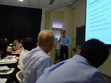
Professor Francois Ladouceur visited GIPO on October 3rd, 2008 (Friday), and lectured in room 113 of Barry Lam Hall. His lecture, “Photonics Material Research at the University of New South Wales” was attended with enthusiasm by GIPO professors and students. Everyone learned much. |
|
|
|
November “Photonics Forum” Lecture
Highlights |
|
Time: |
November 14th, 2008, 4:30 ~ 6:30 pm |
|
Speaker: |
Dr. Tien-Pei Lee {Consultant, University of California, Berkeley; Bellcore, US (retired)} |
|
Topic: |
The Past, Present, and Future of Optoelectronics for Telecommunications – A Personal Reflection |
| |
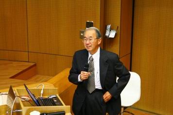
Dr. Tien-Pei Lee visited GIPO on November 14th, 2008 (Friday), and lectured in Auditorium 101, Barry Lam Hall. His lecture, “The Past, Present, and Future of Optoelectronics for Telecommunications – A Personal Reflection” was attended with enthusiasm by GIPO professors and students, and everyone learned much. |
|
|
|
Time: |
November 28th, 2008, 2:30 ~ 4:30 pm |
|
Speaker: |
Professor Ching-Chung Kong
(Researcher, Institute of Atomic and
Molecular Sciences, Academia Sinica)
|
|
Topic: |
The
Synthesis of Single-cycle Optical
Pulses |
| |
Professor Ching-Chung
Kong visited GIPO on November 28th,
2008 (Friday) as a speaker for
Photonics Forum. His lecture, “The
Synthesis of Single-cycle Optical
Pulses”, was attended with
enthusiasm by GIPO professors and
students. Professor Kong’s lecture
was brilliant, and the professor
himself was thorough and
approachable, interacting with his
audience throughout the speech. GIPO
professors and students learned much
from the lecture. |
|
|
|
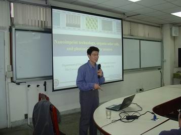
November GIPO Lecture Highlights
|
|
Time: |
November 27th, 2008,
9:30 ~ 10:45 am |
|
Speaker: |
Professor L. Jay Guo (Department of
Electrical Engineering and Computer
Science, University of Michigan, Ann
Arbor, Michigan, USA) |
|
Topic: |
Nanoimprint technology, organic
solar cells, and photonic resonator
sensors |
| |
Professor L. Jay Guo
visited GIPO on November 27th
(Thursday), 2008 and lectured in
Room 142, Electronic Engineering
Building II. His lecture,
“Nanoimprint technology, organic
solar cells, and photonic resonator
sensors” was attended by GIPO
professors and students with
enthusiasm. |
|
|
|
December “Photonics Forum” Lecture
Highlights
|
|
Time: |
December 5th, 2008,
2:30 ~ 4:30 pm |
|
Speaker: |
Prof. Azzedine
Boudrioua (OSA/SPIE fellow,
Université Paris 13 – Institut
Galilée) |
|
Topic: |
Linear and non-linear
photonic crystals in dielectric
materials with applications to
organic LEDs and lasers
|
| |
Professor Azzedine Boudrioua arrived
at GIPO on December 5th
(Friday) 2008, and lectured in Room
113, Barry Lam Hall. His lecture,
“Linear and non-linear photonic
crystals in dielectric materials
with applications to organic LEDs
and lasers” was attended with
enthusiasm by GIPO professors and
students. Everyone learned much from
the lecture. |
|
Time: |
December 12th, 2008, 2:30 ~ 4:30
pm |
|
Speaker: |
Cheng-Hsu Chou (Deputy Director, Chi Mei Optoelectronics Corp.) |
|
Topic: |
The
current state of the
optoelectronics industry and
future career development in
this area |
| |
Deputy Director
Cheng-Hsu Chou visited GIPO on
December 12th (Friday), 2008 as
a lecturer for the Photonics
Forum. His lecture, “The current
state of the optoelectronics
industry and future career
development in this area” drew
enthusiastic participation from
GIPO professors and students.
Deputy Director Chou’s lecture
was exciting and interesting,
with frequent interaction
occurring between the speaker
and his audience. Attending
professors and students learned
much. |
|
 |
|
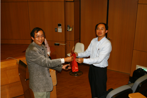
Presider of the forum Professor
Hoang-Yan Lin (left) with Deputy
Director Cheng-Hsu Chou (right) |
|
Highlights from the GIPO 2008 Christmas
Luncheon
Time:
December 24th,
2008
Location: The atrium of Min Da
Hall (3F), College of EECS, National
Taiwan University
Highlights Compilation: Kuang-Chung Liu,
President of the GIPO Student
Association
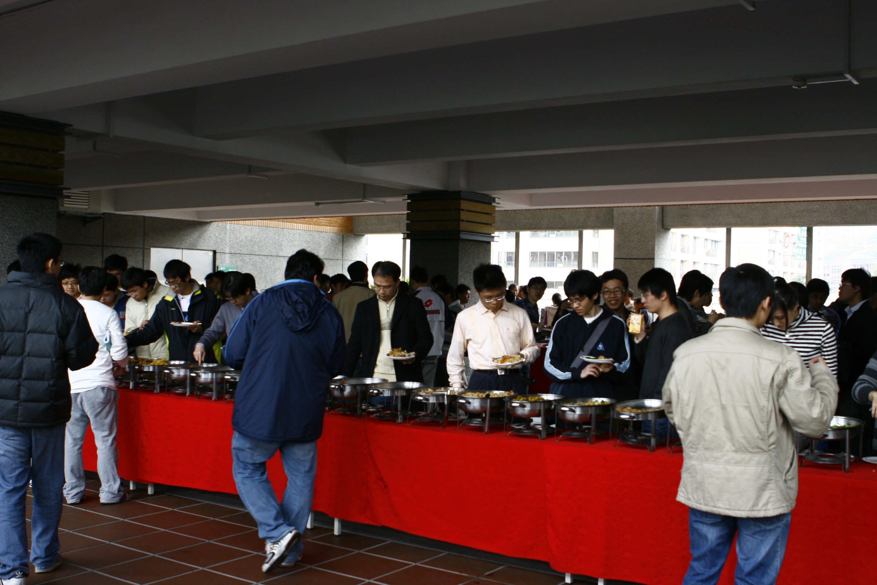
2008 Christmas Luncheon,
sponsored by the GIPO office and GIPO
Student Association was held on December
24th, 2008 at the atrium of Min Da Hall,
3F. Three hundred students and
professors attended, including GIPO
Chairman Sheng-Lung Huang, Professor Lon
A. Wang, Professor Chi-Kuang Sun,
Professor Hoang-Yan Lin, Professor Jian-Jang
Huang, Professor Yuh-Renn Wu, and
Professor Jr Hau He. Scrumptious cuisine
and sweet delicious drinks were
served. In the midst of the fine dining
and merry conversation, the year-end
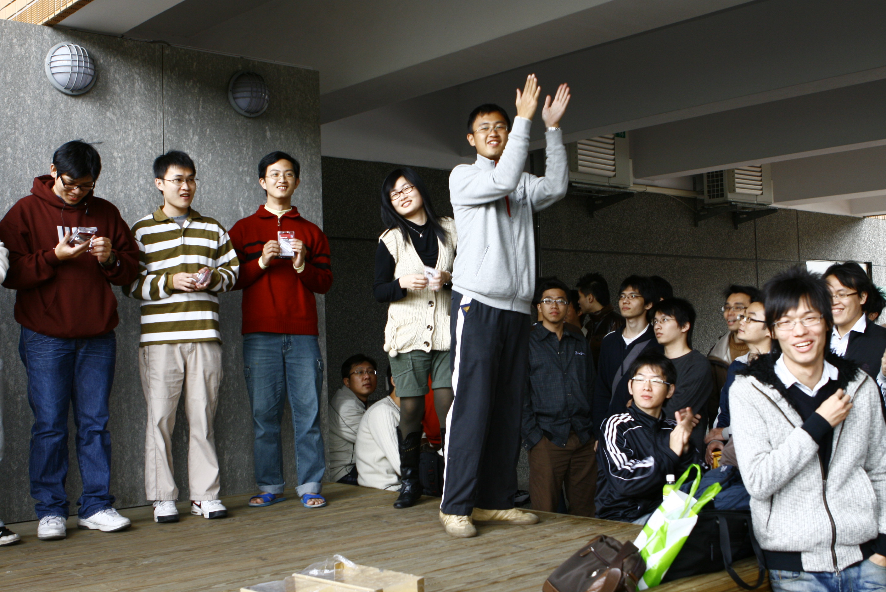
lottery began.
This year’s prizes were
generously provided by the GIPO office
and professors: the grand prize is an
ASUS Eee PC, and 2nd prize is an iPod
Touch. Others include an iRiver, a
Fujitsu high-capacity USB drive,
Transcend 8G and 4G USB drives, and 5000
NT dollars worth of SOGO gift
certificates, provided by Jenn-Gwo Hwu,
Professor and Chairman of the EE
department. Prizes were drawn by the
chairman and professors, and were
equally distributed among laboratories.
After the grand prize was taken by a 1st
year graduate student, the Christmas
party came to a warm and happy close.
Although not everyone walked away with a
prize, we all enjoyed the fabulous lunch
and left with satisfied smiles on our
faces. The Student Association would
like to take this opportunity to thank
the BL312 laboratory (led by Professor
Jian-Jang Huang) for their help in
purchasing prizes, food, drinks; for
renting and decorating of party hall;
and for advertising the luncheon.
|
|
|
|
|
|
| |
|
|
~ An On-Site Visit from the Accreditation
Committee of IEET, Institute of Engineering Education Taiwan ~
Time: October 6th, 2008
Location: Audio-Visual
Room 105, Room 454, and 455, Electrical Engineering Building II,
National Taiwan University
Accreditation Committee Members:
Ching-Ting Lee (Dean, College of Electrical
Engineering and Computer Science, National Cheng Kung University)(Chairman, the Accreditation Committee of IEET)
Cheng-Chung Lee (Professor, Department of Optics
and Photons, National Central University)
Shao-Chung Hsu (Deputy Director, Electronics and
Optoelectronics Research Laboratories, Industrial Technology Research
Institute)
In order to raise the quality of our engineering education and to meet
the standards of international education, GIPO has taken part in the
accreditation program of the Institute of Engineering Education Taiwan
in the 08-09 academic year. On October 6th, 2008, IEET's accreditation
committee visited GIPO and conducted an all-day on-site evaluation in
the Audio-Visual Room 105, Room 454, and 455, Electrical Engineering
Building II. First, the committee members were briefed by the NTU
executive administrators and our chairman, getting to know the
university and this institute. After the briefings, the committee
conversed with the chairman and professors, raising questions about
GIPO’s Self-evaluation Report. The accreditation committee also used
this opportunity to gain a better understanding of GIPO’s curriculum and
the institute’s accomplishments in education. Following, committee
members conversed with 5 alumni representatives, 5 business/industrial
representatives, and 30 GIPO student representatives. These discussions
allowed the committee to better understand how well GIPO graduates
perform post-graduation, how well GIPO forms cooperative relationships
with businesses, and how well current GIPO students perform while they
attend the institute.
After the short lunch break, the accreditation committee held a meeting
to examine the information provided by GIPO, checking that it
corresponds with information given in the institute’s Self-evaluation
Report. Then, accompanied by Chairman Sheng-Lung Huang and Vice Chairman
Gong-Ru Lin, the committee toured GIPO’s educational facilities,
libraries, and laboratories. The committee ended the day's evaluation by
holding a final meeting and announcing its Exit Interview Statement.
The results of the evaluation were announced in March 2009 and our
institute has been successfully accredited. GIPO alumni will be
recognized by members of Washington Accord as having accomplished the
required fundamental education of the engineering profession.
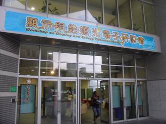
~ Workshop on Display and Energy Optoelectronics ~
Time: October 31st,
2008
Location: Barry Lam Hall, National Taiwan University
Highlights Arrangement: Wen-Ping Chen
The National Innovative Education Program on Image
Display Technology--Center for Display Optoelectronics Technology, a
Ministry of Education project headed by Professor C. C. Yang of GIPO,
hosted “The Workshop on Display and Energy Optoelectronics” on October
31st. The workshop invited 7 domestic professionals from
display technology, solar cells and related fields to lecture. The
lecturers include Associate Professor Wen-Chung Kao, Department of
Applied Electronics, National Taiwan Normal University, on the topic of
“Electrophoretic Display Materials and Flexible E-Paper System Design”;
Group Leader Cheng-Chung Lee, the Display Technology Center, Industrial
Technology Research Institute (ITRI), on the topic of “Flexible TFT and
display technologies and applications”; Manager Pei-Shun Yeh, TPO
Displays Corp., on the topic of “Challenges and Future Trend of AMOLED”;
Assistant Professor Zingway Pei, Department of Electrical Engineering,
National Chung Hsing University, on the topic of “Nanostructure Thin
Film Solar Cell”; Assistant Manager Chih-Yung Hsieh, Technology
Development Center, Chi Mei Optoelectronics, on the topic of “LCD
Display Technology and its Applications: Now and In the Future”;
Assistant Manager Te-Chi Wong, Photovoltaics Technology Center, ITRI, on
the topic of “The Development of High Efficiency Silicon Thin Film Solar
Cell”; and Dr. Yung-Hui Yeh, Electronics and Optoelectronics Research
Laboratories, ITRI, on the topic of “Flexible TFT Technology and
Applications”.
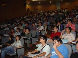
This workshop was made entirely free of charge with the intent of
promoting exchange of information and advancing learning. A large number
of people from different fields attended: 323 people, including GIPO
students, business associates, professors and graduate students from
other universities, high-school teachers, and institute researchers
registered. With such a large number attending, it was necessary to set
up a secondary location in Room 113, Barry Lam Hall in addition to the
main location, Auditorium 101, Barry Lam Hall. Video and audio equipment
was set up in the secondary location to providing access to all
lectures. Lecturers and those attending the workshop interacted well,
and attending students felt they benefitted greatly.
|
The workshop sign-in area
|
Participants attended with
enthusiasm
|
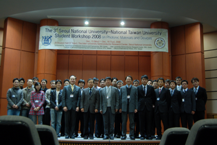
~ The 3rd Seoul National University-National Taiwan University Student
Workshop 2008 on Photonic Materials and Devices ~
Time: December 14th ~
19th, 2008
Location: Seoul National University
Composed by Yu-Chieh Wen, GIPO Ph.D.
candidate
First of all, I would like to thank EECS and GIPO of
NTU for providing me with this opportunity to participate in the NTU and
SNU doctoral student workshop. I’d also like to give special thanks to
GIPO Professor Chi-Kuang Sun and my fellow researchers in our laboratory
for their assistance. The full name of this workshop is “The 3rd
Seoul National University-National Taiwan University Student
Workshop 2008 on Photonic Materials and Devices.” As its name states,
the purpose of this workshop is to provide an opportunity for both
universities' doctoral students to discuss photonic materials and
devices. Upon reading the agenda and realizing that I would interchange
ideas with outstanding scholars and students in the same field, I felt
extremely excited and worked even harder in the hope that our research
results would be even more convincing. Aside from making a clear
presentation of our research to SNU professors and students, we also
learned a great deal about SNU’s development in recent years. I will
describe the experience below.
Doctoral students were the main focus of this
workshop. Students were responsible for giving presentations, hosting,
planning the agenda, and judging presentations. Therefore, the workshop
not only trained students in giving presentations, but also in matters
relating to holding academic workshops. There were 10 presenters from
NTU and 8 from SNU. Each presentation spanned approximately 25 minutes,
including 5 minutes for discussion. The aim of the first twenty minutes
was to give a clear presentation of research achievements in this short
time. If the presenter did so, he would benefit greatly in the last 5
minutes' discussion. After training ourselves to present our research in
20 minutes, we knew our research better, and were better able to grasp
its essence. This new understanding also opens new directions and
possibilities in our own personal research.
In the last 5 minutes of the presentation, the
presenter and the audience discussed the topic. Aside from NTU
delegates, there were also SNU scholars outstanding in research and
experience in these fields. These scholars raised questions and ideas
that were very much worth deeper thought and exploration. For example,
after my presentation on optical thin film measurement, SNU’s Professor
Yoon asked me a question about the surface roughness and efficiency of
LED components. These are questions that have received a lot of
attention of late in this field. Another question that was raised
concerned the propagation depth of acoustic waves. This question hit the
proverbial nail on the head, and cut straight to the limitations of this
experimental technology, giving me an opportunity to clarify some
confusion the audience might have felt. Aside from formal discussion, we
could also discuss our research with other scholars and students after
the presentation. Although these informal discussions might not directly
contribute any groundbreaking ideas, they did reveal how clear or
ambiguous our presentations were, making this event an excellent
experience in learning how to participate in academic exchange in a
clear manner.
Aside from giving our own presentations, listening to
others was also a quick way to understand recent developments in related
fields. In these presentations, it was common to find research
achievements which had recently been published in top international
journals. Since the workshop focused on academic exchange, students
often introduced the research of their laboratories. These introductions
allowed us to understand not only the specialty of each laboratory, but
also the perspective of the whole field. Attending the workshop for
those two days allowed me to gain a better understanding of photonics
research in general. I’ve realized the importance of knowing about the
general development of related fields. Aside from finding the right
direction for our own research, we have to understand where the main
points of the research are. This way, when publishing our research, we
will better understand what readers may not know and can better explain
these points. The English speaking abilities of both NTU and SNU
students are about equal. However, it was clear that SNU students
invested a lot of effort in producing and developing their powerpoint
presentations, which is something we may improve on in the future.
Presentations were the focus of the workshop, but
there were still breaks and meal times during the day. During these
times, while everyone was eating lunch or snacking and drinking coffee,
it was common to see groups of people gathered together to chat and
further discuss their research. Of course, there were also people who
approached me after my presentation to talk about my research. In fact,
I feel that breaks and meal times were an excellent time to socialize
and learn. Over the course of this workshop, I met many professors, and
exchanged ideas with numerous SNU students, all of which will greatly
benefit my research in the future. Therefore, during breaks, I made
efforts to socialize with professors and other students. However, due to
limited language skills, these conversations often did not flow
smoothly. This experience has allowed me to further realize the
importance of an ability to communicate in English. Although I can speak
some English, I am not fluent enough to use it to my advantage in a
social setting. In addition to speaking English, conveying ideas
on-the-spot is also important. I believe that even if speaking in
Chinese, I may not be able to convey my ideas in a clear and simple
manner. Although I am not satisfied with my performance in socializing
with others during break times, I have at least taken the first step,
and will strive to improve myself.
It
has been a rare and invaluable experience to attend the exchange with
SNU. I would like to thank EECS and GIPO, NTU, for their sponsorship
which allowed us to attend this workshop. During the workshop, I came
face to face with top experts in related fields. This experience has
expanded my world view, gradually built my confidence in my research,
and allowed me to better understand what I have achieved so far. Having
been through this experience, I expect not only to make significant
breakthroughs in my research, but also to improve my ability to
socialize and exchange on an international level.
|
 |
|
Workshop participants |
|
|
|
|
|
|
|
| |
|
|
|
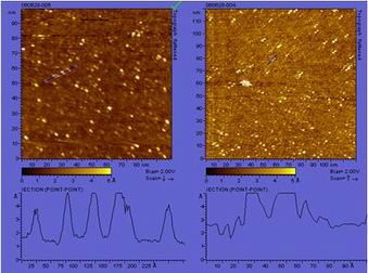
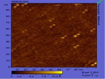
Nanostructures of Organic Light Emitting Materials
Professor
Chih-I Wu
Graduate Institute of
Photonics and Optoelectronics, National Taiwan
University
In the previous year, we have been working on the investigation of the arrangement and orientation of the organic thin films deposited on various surfaces. We have probed the organic molecular arrangement at the substrate in nano-scale with scanning tunneling microscope (STM). We deposited less than 0.1 mono-layer of NPB on silicon surface and investigate with STM. As shown in Figure 1, the NPB molecules can be seen clearly as the bright spots on the surface. The NPB molecules are evenly spread on the surface of the substrate. More amazingly, some of the molecules are form as dimers as shown in the Figure 2. The underlying interaction and physics of the formation of the dimers will be investigated this year.
We also perform the photoelectron emission microscopy (PEEM) at National Synchrotron Radiation Research Center (NSRRC) to investigate the orientation of the organic electronic films on different substrates. From the spectra we can determine that CuPc molecules lie flatly on the Au surfaces, whereas the same molecules arrange perpendicular to the ITO surface with the same deposition condition. The result demonstrate that we can use PEEM to determine the stacking arrangement of the organic molecules at the surfaces with PEEM, which can be a good complement technology to STM and very useful to the nanotechnology projects.
|
|
 |
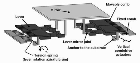
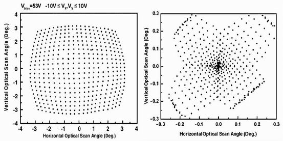
Linearization
of a Two-Axis MEMS Scanner Using a Differential Driving
Scheme
Professor Jui-che Tsai
Graduate Institute of
Photonics and Optoelectronics, National Taiwan
University
A driving scheme using
a pair of differential voltages (Vx,
Vy) over a bias voltage is proposed to linearize the dc characteristic (angle versus voltage) of a two-axis MEMS scanner. The micromirror has a gimbal-less structure and is driven by vertical comb-drive actuators in conjunction with a leverage mechanism (Figure 1). At an optimal bias voltage of 53 V, a linear optical scan range of ±3.2 deg. is achieved experimentally in both the x and y directions with the differential voltages ranging from −10 V to + 10 V (Figure 2, left).
For comparison, a non-differential driving scheme with two independent voltages, Vx
and
Vy, is implemented (Figure
2, right). In our experiment,
Vx
and
Vy
both vary from 0 to 16.5 V with an increment of 1.65 V. It can be seen that the pattern is profoundly distorted even with a small optical scan range of <±0.3 deg. The slight asymmetry is due to optical system misalignment and the non-uniformity among levers.
|
Figure 1. Schematic of the two-axis MEMS scanner
driven by vertical comb-drive actuators in
conjunction with a leverage mechanism. |
|
 |
|
Figure 2. Scan patterns of differential (left) and non-differential (right) driving. |
|
© 2008 Institute of
Physics (IOP) and IOP Publishing Ltd
J. C. Tsai et al.,
“Linearization of a two-axis MEMS scanner
driven by vertical comb-drive actuators,”
J. Micromech. Microeng., Vol. 18, No. 1,
015015, Jan. 2008.
|
Temperature-Dependent Stability of On-Plastic a-Si:H
Thin Film Transistors
Professor I-Chun Cheng's group
Graduate Institute of
Photonics and Optoelectronics, National Taiwan
University
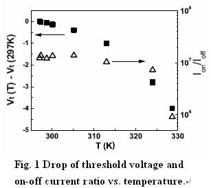
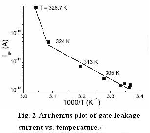
We investigated the temperature-dependent stability on the inverted-staggered back-channel-etched a-Si:H thin film transistors (TFTs) made at a process temperature of 150°C on plastic foil substrates. The shift of threshold voltage (Vt) increases with the stressing time and the stressing temperature. Different from TFTs made at temperatures of 300 °C or above, our low-temperature processed TFTs show an abnormal saturation of Vt at 50°C (323 K) in a constant gate-bias stress experiment. Around the same temperature, we observed abrupt increases in both the gate leakage current and the off current. Because of the low process temperature, the gate dielectric is less stable and more defective compared to that made at high process temperatures. A substantial amount of charges, trapped inside the dielectric during TFT fabrication and gate-bias stressing, was thermionically emitted into the channel by the Poole–Frenkel emission mechanism at a stressing temperature of 50°C, leading to the abnormal phenomena.
|
|
 |
|
Analyzing the
Optical Phase Conjugation Phenomenon via
PSTD Simulations
Professor Snow H.
Tseng
Graduate Institute of Photonics and Optoelectronics,
National Taiwan University
Turbidity Suppression via Optical Phase
Conjugation is an optical phenomenon
that uses the back propagation nature of
optical phase conjugate light field to
undo the effect of tissue scattering.
We use the computationally efficient and
accurate pseudospectral time-domain (PSTD)
simulation method to study this
phenomenon; a key adaptation is the
volumetric inversion of the optical
wavefront E-field as a means for
simulating a phase conjugate mirror.
Optical phase conjugation (OPC)
phenomenon of a phase conjugate mirror
may provide a means to disentangle the
optical distortion caused by scattering
of turbid media.
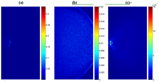
As shown in Fig. 1, PSTD simulation of
light scattering through a macroscopic
cluster of dielectric cylinders and
reflected back by a PCM is shown. After
OPC, light back-traces and refocuses
back to the original location where it
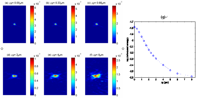
first emerged. Displacement effect (Dy)
of the random media is further analyzed
and shown in Fig. 2. The refocused
light pulse profile for random medium
that is displaced by various
Dy is shown
in (a)-(f). The ratio of the total
refocused energy to the initial total
energy for various
Dy is shown on a
semi-log scale in (g). Notice that as
Dy increases, the refocused light energy
drops rapidly.
The PSTD simulation is a rigorous
simulation technique capable of
simulating light scattering phenomenon
for large-scale problems. Our
simulation results provide important
information to experiments to help
understand the optical characteristics
of OPC.
|
 |
|
Fig. 1. PSTD
Simulation of OPC. |
 |
|
Fig. 2. The
displacement effect of the random medium
on the OPC phenomenon. |
Etching Depth
Dependence of Emission Properties from
InGaN/GaN Light Emitting
Diodes with
Nanohole Arrays: Analysis of Strain
Relaxation and Surface States
Professor Yuh-Renn Wu
Graduate Institute of Photonics and
Optoelectronics, National Taiwan
University
We apply our simulation models to
analyze the etching depth dependence of
emission characteristic of the InGaN/GaN
quantum well. The effect of strain
relaxation and surface states are
discussed in this work. The device
structures are shown in Fig. 1(a).
Figure 1(b) and 1(c) show the strain
tensors
εxx
with the hole depth equal to
16 nm and 23 nm, respectively.
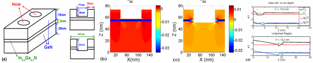 |
|
Fig. 1
(a) A schematic of the nanohole
structure. The hole depths are 16nm and
23nm. (b) and (c) show the calculated
strain tensor
εxx
of the nanohole structure with 16nm hole
depth and with 23nm-column hole depth,
respectively. (d) shows the band
structures and wavefunction of 16 nm
nanohole structure at X=73.6nm and
X=10.2nm, respectively. |
As the strain data shown in Fig. 1, the
nanohole structure with 23 nm hole depth
might have a larger blue shift due to
the strain relaxation. In 16 nm hole
depth cases, because of the effect of
surface states at the air/GaN interface,
the fermi level is usually pinned at the
surface states level (~ 0.9eV below
conduction band for GaN). If the cap
layer is thick enough, the effect of the
surface states is negligible. However,
the distance from the surface state to
the quantum well region is only 2 nm in
the cases. The pinning position of the
surface state will strongly affect the
band bending of the cap layer and the
InGaN quantum well layer. When the top
GaN layer is too thin as shown in Fig. 1
(d), the band bending at the GaN layer
is not large enough so that potential at
the left side of InGaN quantum well is
lifted up, which reduces the QCSE
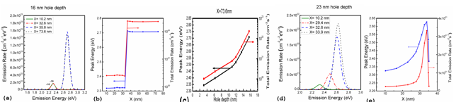
significantly. Figure 2(a) shows the
calculated emission spectrum at
different position of the nanohole. Due
to the surface states pinning effect,
our results show that the emission rate
is enhanced by 82 times and the maximum
of 380 meV blue shift compared to the
unetched region. The etched and unetched
areas have a significant difference in
the emission properties in Fig. 2(b). We
can also find that for the hole depth
larger than 11 nm (~ 7nm to the quantum
well), the emission rates and emission
peak start to have a significant change
in Fig. 2(c). At X = 33.9 nm, the strain
relaxation of quantum well and the
emission rate reaches the maximum as
shown in Fig. 2(d). Fig. 2(e) shows the
emission peak and emission rates versus
different positions X. The emission
property of the nanohole changes
significantly when the hole depth is
close to or penetrates the quantum well.
One is due to the effect of surface
states and the other one is due to the
strain relaxation.
 |
|
Fig. 2
(a) shows the calculated emission
spectrum. The emission spectrum at $X$
=10.2 nm and 32.6nm is multiplied by 10
times to make them clear. (b) shows the
total emission rate and the emission
peak energy versus different positions
for the 16 nm nanohole structure. (c)
The calculated emission strength and
emission peak energy versus different
hole depth. (d) shows the calculated
emission spectrum of the 23 nm nanohole
structure, and (e) shows the emission
peak energy and the total emission rate
versus different positions for the 23 nm
depth nanohole structure. |
In conclusions, we have analyzed the
emission characteristic of InGaN/GaN LED
with depth dependence of the nanohole
structure. The emission property of the
nanohole changes significantly when the
hole depth is close to or penetrates the
quantum well. One is due to the effect
of surface states and the other one is
due to the strain relaxation. Both
effects lead to the blue shift of the
spectrum and the increase of radiation
recombination rates so that it is hard
to be directly determined from
experimental PL measurement. Our
calculation provides useful information
for analyzing the spectrum shift in the
nanohole array and would be very
important factors to be considered when
making these similar structures such as
nanocolumns and nanorods.
Electrical and
Optoelectronic Characterization of a ZnO
Nanowire Contacted by
Focused-Ion-Beam-Deposited Pt
Professor J. H. He
Graduate Institute of Photonics and
Optoelectronics, National Taiwan
University
We
report on the transport properties of
single ZnO nanowires measured as a
function of the length/square of radius
ratio via transmission line method. The
specific contact resistance of the FIB
Pt contacts to the ZnO nanowires is
determined as low as
1.1x10⁻⁵
Ωcm2. The
resistivity of the ZnO nanowires is
measured to be
2.2x10⁻²
Ωcm. ZnO
nanowire-based UV photodetectors
contacted by the FIB-Pt with the
photoconductive gain as high as ~108
have been fabricated and characterized.
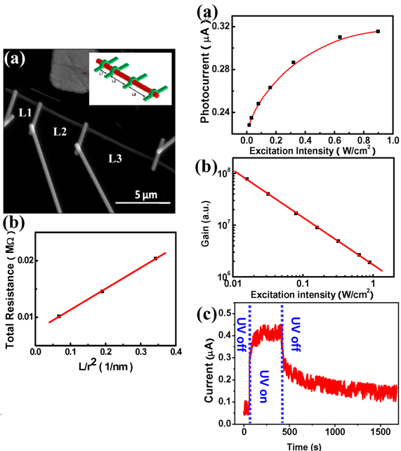 |
|
Figure 1. (a) SEM image of the test structure of
TLM measurement. (b) Total resistance as
a function of the length over the square
radius of ZnO NW.
Figure 2. (a) Photocurrent measurement as a
function of excitation power intensity
at applied bias of 0.5 volt. (b)
Photoconductive gain as a function of
excitation power intensity. (c)
Time-dependent photocurrent rise and
decay as obtained by sudden application
(at 60 s) and removal (at 400 s) of UV
light at the bias of 0.5 volt. |
|
|
|
|
|
|
| |
|
|
 |
|
 |
|
|
|