Latest News Special Report Research Result Column Profiles Laboratory Descriptions
![]() Congratulations! GIPO Distinguished Research Fellow Chen-Shui
Tsai was awarded Chancellor Professorship at UC Irvine.
Congratulations! GIPO Distinguished Research Fellow Chen-Shui
Tsai was awarded Chancellor Professorship at UC Irvine.
|
Dr. Chen-Shui Tsai, Distinguished Research Fellow, received Chancellor Professorship at UC Irvine. Congratulations! In order to attract outstanding professors and scholars, the UC system has established the honorable position of Chancellor Professorship. 18 professors out of nearly 2000 from of the UC Irvine area were awarded this honor. |
 |
![]() Congratulations! Professor Gong-Ru Lin is selected as the
2008 SPIE Fellow.
Congratulations! Professor Gong-Ru Lin is selected as the
2008 SPIE Fellow.
|
GIPO Vice Chairman Gong-Ru Lin was selected as the 2008 SPIE Fellow, and became one of the 72 new members of the said society. Congratulations! Every year, SPIE (The International Society for Optical Engineering) selects scholars who have made important contributions to the optoelectronics research to receive this honor. Vice Chairman Gong-Ru Lin was honored as a 2008 SPIE Fellow for his specific achievements in fiber lasers and silicon nanophotonics. For details and related information, refer to the following website: http://spie.org/x32.xml. |
 |
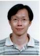
![]() Congratulations! Professor Chung-Chih Wu is awarded the 21st
Khwarizmi International Award (KIA).
Congratulations! Professor Chung-Chih Wu is awarded the 21st
Khwarizmi International Award (KIA).
|
GIPO Professor Chung-Chih Wu has been awarded the 21st Khwarizmi International Award (KIA) for his outstanding work on fusing solar cells and advanced OLED technologies. Congratulations! For more information, refer to the following website: http://gipo.ntu.edu.tw/200804/KIA.htm. |
 |
![]() GIPO
Academic
Visiting
Highlights
GIPO
Academic
Visiting
Highlights
|
March “Photonics Forum” Lecture Highlights |
|
|
Time: 4:00~6:00 pm, March 7th, 2008 Speaker: Dr. J. T. Lin (Director, New Vision, Inc., Visiting professor, NCTU; Consultant, Laser Application Technology Center, ITRI; Consultant, Hon-Hai Technology Group) Topic: Recent Progress in Medical Laser Technologies Dr. J.T. Lin visited GIPO on March 7th, 2008, and spoke in conference room 101, Barry Lam Hall. His lecture, “Recent Progress in Medical Laser Technologies” was attended with enthusiasm by GIPO professors and students, and all the participants learned much from the lecture. |
|
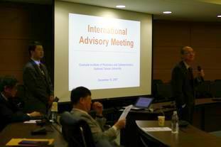
![]() 2007 academic year GIPO Advisory Committee Meeting
2007 academic year GIPO Advisory Committee Meeting
![]()
Saturday, December 15, 2007
Barry Lam Hall, Rm 201, College of EECS, NTU
Committee Members:
Prof. Yung-Sheng Liu, Chair (National Tsing Hua Univ.)
Prof. Connie Chang-Hasnain (U. C. Berkeley)
Prof. Soo-Jin Chua (National Univ. of Singapore, Singapore)
Prof. Silvano Donati (Pavia Univ., Italy)
Prof. Hiromasa Ito (Tohoku University)
Prof. Shin-Tson Wu (Univ. Central Florida)
Dr. Biing-Seng Wu (Executive Vice President of Chi Mei Optoelectronics Corp.)
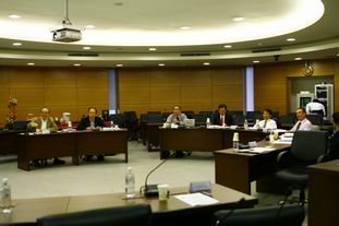
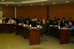
The biennial GIPO Advisory Committee Meeting took place on December 15 in the Barry Lam Hall, room 201. For this grand occasion, seven renowned scholars and experts were invited to join the advisory committee and provide valuable suggestions for improvement. The event sparked great enthusiasm, with 25 professors attending. Each professor presented their own research and responded to suggestions from the visiting committee members. The event began at 9 am and ended at 9 pm. As the end of the year 2007 drew near, the successful Advisory Committee Meeting provided a wonderful demonstration of the progress GIPO had made in the past two years, and brought the year to a brilliant ending.
This year, we were fortunate to have Dean Pei, who took time from his busy schedule, speak at the opening ceremony, and Chairman Huang reported on GIPO’s current state and gave a short introduction of the institute. Following the summary, GIPO professors each provided a briefing on their own research. Time was also arranged for committee members to meet GIPO professors and student representatives separately in order to discuss current GIPO issues and exchange ideas. Finally, after the committee members convened to discuss their views, Dr. Yung S. Liu, the Chair of the committee summarized the committee’s suggestions and the meeting came to a successful conclusion.
To recompense the committee members and professors who sacrificed their weekend and spent the day in the meeting, GIPO arranged a sumptuous dinner banquet. Members and professors continued their discussions while enjoying their delicious meal. President Si-Chen Lee was especially invited, and his attendance made the banquet even more special, drawing this year’s Advisory Committee Meeting to a perfect close.
 |
 |
|
Dean Soo-Chang Pei, College of EECS (above) speaking. |
Seven advisory committee members listened closely and exchanged ideas. |
 |
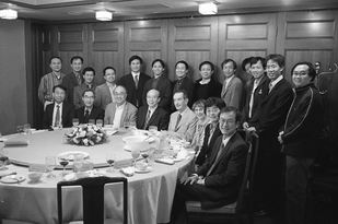 |
| GIPO professors attended with great enthusiasm. | President Lee attended the dinner banquet, and was photographed with committee members and GIPO professors. |
![]() 2007 Taiwan-Russian Joint Symposium on Nanostructures and Nanoelements
2007 Taiwan-Russian Joint Symposium on Nanostructures and Nanoelements
for Photonics and Optoelectronics Applications
![]()
November 21st to 22nd, 2007
Barry Lam Hall, Room 201, National Taiwan University
Highlights Compilation: GIPO graduate students I-Ning Hu, Han-Min Wu
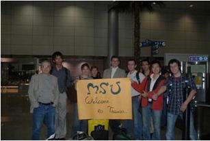
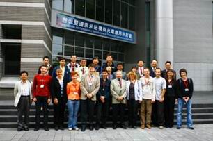
The 2007 Taiwan-Russian Joint Symposium on Nanostructures and Nanoelements for Photonics and Optoelectronics Applications took place on November 21st and 22nd. The workshop, hosted by GIPO professor Lung-Han Peng and the research fellow Andy Kung of the Institute of Atomic and Molecular Sciences, Academica Sinica, was held on an Autumn morning at Barry Lam Hall, Room 201. Chairman Panov, Department of Physics, M. V. Lomonosov Moscow State University (MSU), and President Sigov of Moscow State Technical University of Radio Engineering, Electronics and Automation (MIREA) headed a visiting group of 7 scholars and 6 doctorate students from related fields. Aside from sharing advancements made in nano technology research, the workshop also focused on academic exchange, and signing the Academic Exchange Agreement between the Department of Physics, M. V. Lomonosov Moscow State University (MSU), and GIPO, National Taiwan University. Doing so should increase future academic and research exchange between both parties, allowing NTU and Russian students a chance to internationalize and increase their competitiveness.
 |
 |
|
Russian scholars were welcomed with giant posters at the Taiwan Taoyuan International Airport. |
Taiwanese and Russian scholars in front of Barry Lam Hall. |
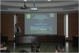
Professor Lung-Han Peng hosted the opening ceremonies on the first day, introducing the attending academics and professors from Taiwan and Russia. Next, Professor Mishina of MIREA and Chairman Panov of MSU introduced MIREA and MSU respectively, describing their histories, campuses, also reporting on recent and future developments in research. Both universities have made advancements of considerable depth in several popular research fields. Following the introductions, Professor C. C. Yang of GIPO spoke on the research advancements GIPO had made in recent years. Professor Yang has extensive knowledge of this subject matter, and his introduction of NTU and GIPO was interesting and informative. Professor Yang’s speech allowed the Russian students to get to know National Taiwan University’s long-standing history, and gain a better understanding of GIPO’s research.
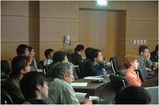
Over the two days of the workshop, the majority of Russian scholars spoke in the morning, while afternoons were dedicated to renowned Taiwanese professors in the nano field. Attending professors included Professor Jin-Hua Huang of the Department of Materials Science and Engineering, National Tsing Hua University; Professor Shing-Chung Wang of the Department of Photonics, National Chiao Tung University; Professor Shoou-Jing Chang of the Department of Electrical Engineering, National Cheng Kung University; Professor Jen-Inn Chyi of the Department of Electrical Engineering, National Central University; Professor Tsong-Sheng Lay of the Institute of Electro-Optical Engineering, National Sun Yat-sen University, Professor Ray-Hua Horng of the Institute of Precision Engineering, National Chung Hsing University; Professor Dong- Shing Wuu of the Department of Materials Science and Engineering, National Chung Hsing University; Professor Yi-Chia Chen of the Department of Materials Science and Engineering, National Dong Hwa University; and Professor Chia-Liang Cheng of the Department of Physics, National Dong Hwa University. The participating professors from National Taiwan University were Professor Chih-Fuh Lin, Professor Yun-Li Li, Professor Jr-Hau He, Professor Hung-Chun Chang, Professor Gong-Ru Lin, Professor Snow H. Tseng, Professor Zhe-Chuan Feng, Professor Guo-Dung Su, Professor Jiun-Haw Lee, Professor Yuh-Renn Wu, and Chairman Jer-Ren Yang, Department of Materials Science and Engineering. The professors reported on their own research findings, and it was clear that each strove hard to further develop nanostructures research; one remarkable report followed another. The discussions that took place after the reports were also intense and energetic. This year’s meeting and exchange thoroughly satisfied each and every participant’s thirst for knowledge.
 |
 |
|
Professor Mishina provided an introduction for MIREA. |
The participants listened with close attention. |
On November 23rd, President Sigov of MIREA and Chairman Panov of Department of Physics, MSU met with President Si-Chen Lee, NTU, to discuss the exchange between each university. During the meeting, the parties reached several agreements, establishing a firm foundation for formal exchanges between the universities in the future. These agreements will benefit students from both Taiwan and Russia, increasing exchange, collaboration, and also promoting high-tech research and development.
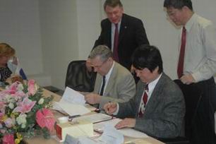
Next, Chairman Panov of Department of Physics, MSU, and Chairman Sheng-Lung Huang of GIPO, NTU, signed an academic exchange agreement, with Deputy Dean Yanwing Leung of the Office of International Affairs, NTU, and President Sigov of MIREA as witnesses. This agreement promotes future academic exchange between GIPO of NTU, MSU, and MIREA. It is also a milestone in the establishment of a cooperative relationship between NTU, MSU and MIREA, and is one of the most important achievements of this Taiwan-Russia workshop.
|
|
|
|
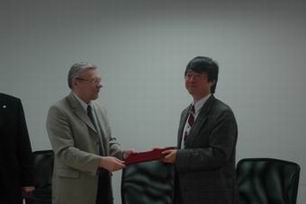
Chairman Panov of Department of Physics, MSU, and Chairman Sheng-Lung Huang of GIPO, NTU, signed the exchange agreement. |
|
![]() The 5th Workshop on Fibers and Optical Passive
Components
The 5th Workshop on Fibers and Optical Passive
Components
![]()
December 5th to 7th, 2007
Barry Lam Hall, National Taiwan University
Highlights Compilation: Wen-Ping Chen
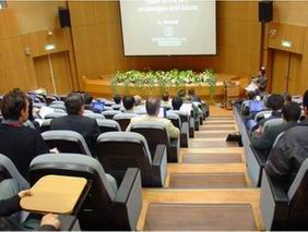
The 5th Workshop on Fibers and Optical Passive Components, organized by GIPO Professor C. C. Yang, Professor Hung-Chun Chang, and Professor Gong-Ru Lin, successfully took place on December 5th to 7th at Barry Lam Hall. This year’s workshop marked the first time for the event to be moved from Europe, hosted in Asia. Participants chose from 14 sessions, each with a different topic, according to his or her own research interests. The specially invited plenary speakers were Professor Masataka Nakazawa from Japan, and Professor Lorenzo Pavesi from Italy, both of whom have impressive reputations in their research fields. In addition to the two plenary speakers, 18 other speakers from Australia, Italy, U.S.A., Canada, Belgium, Hong Kong, Korea, and Singapore were invited to present their papers. Scholars from all circles of society signed up with enthusiasm. In total, 55 oral papers and 24 poster papers were presented. Aside from GIPO professors and students, participants also included members of the industrial circle, professors and graduate students from other universities, and members of research institutions.
After the conclusion of the plenary sessions on the first day of the workshop, a photo session was organized in front of Barry Lam Hall to capture this rare and momentous occasion. The welcome reception on December 5th was held at the Forte Oliver Garden, Ming-Da Hall, while the dinner banquet on December 6th was held at Café 83, Leader Hotel. Our guests from all over the world exchanged research ideas while enjoying the relaxing atmosphere and delicious cuisine. The workshop allowed students and professors to familiarize themselves with recent developments in this field, and also better understand the direction of future development.
|
|
|
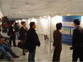
| Participants are numerous and enthusiastic. |
Poster paper exhibit. |
![]() Report on GIPO, National Taiwan University Visit
Report on GIPO, National Taiwan University Visit
to Renown Universities and Research Institutes in China
![]()
March 8th to 16th , 2008
In April of 2007, Professor C. C. Yang headed a party to visit Peking University, Tsinghua University, Nanjing University, and Institute of Semiconductors, Chinese Academy of Sciences (CAS) and Institute of Physics, CAS. All the participants learned much from this visit. This year, Professor Yang once again assembled a party to visit other prominent schools in China, including Zhe Jiang University, Shanghai Jiao Tong University, Shanghai Institute of Optics and Fine Mechanics (SIOM), CAS, Fudan University, East China Normal University, Suzhou Institute of Nano-tech and Nano-bionics, CAS, Suzhou Industrial Park, and Soochow University. The members of the visiting party include Chairman Sheng-Lung Huang, Vice Chairman Gong-Ru Lin, Professor Zhe-Chuan Feng, Professor Cheewee Liu, Associate Professor Chih-I Wu, Assistant Professor Snow H. Tseng, Assistant Professor Yun-Li Li, Assistant Professor Jr Hau He, and GIPO Newsletter Editor Ms. Hsiao-Wen Lin. The ten members of the party set off on March 8th and began a tightly-scheduled visit of nine days. The party members learned much from this visit, and were astonished at the incredible speed with which China’s prominent educational institutes and research centers progressed.
![]() Research Result Column for the Program of
“Aiming for Top University”
Research Result Column for the Program of
“Aiming for Top University”
Calculating Decay Rate of Finite Size Photonic Crystal Waveguides
Professor Yih-Peng Chiou
Graduate Institute of Photonics and Optoelectronics, National Taiwan University
In recent years, photonic crystals (PhC) have attracted a lot of attention due to their exotic properties. By applying the properties, many applications have been proposed, such as filters, waveguides, cavities, beam splitter, etc. To design those devices, an effective numerical method is required. The plane wave expansion method (PWEM) based on Fourier series expansion is frequently adopted. However, it can only be applied to devices made by lossless and dispersionless materials. In addition, it can not analyze the leakage due to finite-size structures. However, in reality, devices cannot be made infinitely, and guided waves may suffer from significant leakage due to finite periodic structures.
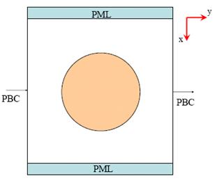
We have derived a modified finite-difference method from Maxwell’s equations to calculate wavevectors corresponding to a certain given frequency. The above-mentioned limitations with conventional PWEM are overcome. We apply the developed method to analyze the propagation phenomena of finite-size photonic waveguides. Finite-difference method combined with perfect match layers (PML) are adopted in the analysis.
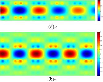
Fig. 1 shows the calculation domain. Fig. 2 shows the mode patterns of PhC waveguides with (a) one unit cell and (b) three unit cells beside the line defects. It can be seen that the decay is significantly reduced as more unit cells are added beside the line defects.
 |
 |
|
Fig. 1 Representation of calculation domain. |
Fig. 2 Mode pattern of PhC waveguides with (a) one unit cell and (b) three unit cells beside the line defects. |
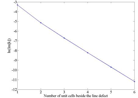
The decay rate and the number of unit cells beside the line defects is linear in semi-logarithmic diagram as shown in Fig. 3, where k is the calculated propagation constant.
 |
|
Fig. 3 The relation between number of unit cells beside line defect and decay rate. |
![]()
![]()
ZnS/Silica Nanocable Field Effect Transistor as Biological and Chemical Nanosensors
Professor Jr Hau He
Graduate Institute of Photonics and Optoelectronics, National Taiwan University
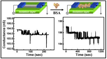
Sensing using planar field effect transistor (FET) has been demonstrated for decades but lower sensitivity has limited its applications. Compared to the surface region of a planar device, due to the ultrahigh surface-to-volume ratio, NWs and carbon nanotubes (CNTs) are ideal choices for sensors due to the introduced depletion/accumulation of charges near the surface as a result of surface binding/adsorption of foreign molecules and species. The NWs that have been extensively developed for sensing are silicon because of the massive knowledge that has existed for the chemical modification of native Si oxide surfaces. The FET of ZnS/silica core/shell nanostructures are attractive to biological and chemical sensors due to (i) its excellent and reproducible electronic characteristics of ZnS, (ii) the self-assembled silica shell as natural insulator on the surface of ZnS NW that serve as the protection layer against oxidation, and (iii) the massive existing knowledge about the chemical modification of silica surfaces.
Compound semiconductor/isolator (ZnS/silica) core/shell nanocables have been used to fabricate single nanowire based field effect transistors, which have been used for label-free, real-time, and sensitive detection of biological species. After chemical modification, amine- and oxide-functionalized nanocables exhibit linear pH-dependent conductance, which could be elucidated in terms of the change of surface charge during protonation and deprotonation.
|
|
|
Figure 1. Real-time detection of non-specific binding of protein. Schematic diagram of a nanocable FET configured as a sensor: binding of BSA with net negative charge yields a decrease in the conductance. |
|
|
![]()
![]()
Advanced Numerical Modelling for Photonic-Crystal and Optical-Waveguide Structures
Professor Hung-Chun Chang
Graduate Institute of Photonics and Optoelectronics, National Taiwan University
A novel analysis method based on a multidomain pseudospectral method is proposed for calculating the band diagrams of two-dimensional photonic crystals and is shown to possess excellent numerical convergence behavior and accuracy. The proposed scheme utilizes the multidomain Chebyshev collocation method. By applying Chebyshev-Lagrange interpolating polynomials to the approximation of spatial derivatives at collocation points, the Helmholtz equation is converted into a matrix eigenvalue equation which is then solved for the eigen frequencies by the shift inverse power method. Suitable multidomain division of the computational domain is performed to deal with general curved interfaces of the permittivity profile and field continuity conditions are carefully imposed across the dielectric interfaces. The proposed method shows uniformly excellent convergence characteristics for both the transverse-electric and transverse-magnetic waves in the analysis of different structures. The analysis of a mini band gap is also shown to demonstrate the extremely high accuracy of the proposed method. (Physical Review E, vol. 75, pp. 026703-1–026703-14, 20 February 2007.)
New full-vectorial optical waveguide eigenmode solvers using pseudospectral frequency-domain (PSFD) formulations for optical waveguides with arbitrary step-index profile are presented. Both Legendre and Chebyshev collocation methods are considered in the formulation. By applying Legendre-Lagrange or Chebyshev-Lagrange interpolating polynomials to the approximation of spatial derivatives at collocation points, the Helmholtz equations for the transverse-electric or transverse-magnetic components are converted into a matrix eigenvalue equation which is then solved for the eigenmodes by the shift inverse power method. Suitable multidomain division of the computational domain is arranged to deal with general curved interfaces of the refractive-index profile together with a curvilinear mapping technique for each subdomain so that field continuity conditions can be carefully imposed across the dielectric interfaces, which is essential in achieving high numerical accuracy. The solver is applied to the optical fiber for the assessment of its numerical performance, to the classical benchmark rib waveguide for comparing with existing high-accuracy results, and to the fused fiber structure for demonstrating its robustness in calculating the form birefingence. (IEEE Journal of Quantum Electronics, vol. 44, no. 1, pp. 56–66, January 2008.)
A finite element method based eigenvalue algorithm is developed for the analysis of band structures of two-dimensional non-diagonal anisotropic photonic crystals under the in-plane wave propagation. The characteristics of band structures for the square and triangular lattices consisting of anisotropic materials are examined in detail and the intrinsic effect of anisotropy on the construction of band structures is investigated. We discover some interesting relationships of band structures for certain directions of the wave vector in the first Brillouin zone and present a theoretical explanation for this phenomenon. The complete band structures can be conveniently constructed by means of this concept. (Optics Express, vol. 15, no. 9, pp. 5416–5430, 30 April 2007.)
A full-vectorial finite element method based eigenvalue algorithm is developed to analyze the band structures of two-dimensional (2D) photonic crystals (PCs) with arbitray 3D anisotropy for in-plane wave propagations, in which the simple transverse-electric (TE) or transverse-magnetic (TM) modes may not be clearly defined. By taking all the field components into consideration simultaneously without decoupling of the wave modes in 2D PCs into TE and TM modes, a full-vectorial matrix eigenvalue equation, with the square of the wavenumber as the eigenvalue, is derived. We examine the convergence behaviors of this algorithm and analyze 2D PCs with arbitrary anisotropy using this algorithm to demonstrate its correctness and usefulness by explaining the numerical results theoretically. (Optics Express, vol. 15, no. 24, pp. 15797–15811, 26 November 2007.)
![]()
![]()
White-light light-emitting device based on surface plasmon-enhanced CdSe/ZnS nano-crystal wavelength conversion on a blue/green two-color light-emitting diode
Professor C. C. Yang’s Group
Graduate Institute of Photonics and Optoelectronics, National Taiwan University
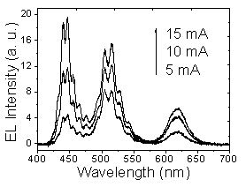
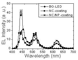
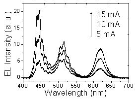
We demonstrate the implementation of a white-light device by spin-coating CdSe/ZnS nano-crystals (NCs) on the top of a blue/green two-color InGaN/GaN quantum-well light-emitting diode for converting blue and green emissions into red light through the absorption/reemission process. Meanwhile, Au nano-particles (NPs) are mixed with CdSe/ZnS NCs for generating localized surface plasmon (LSP) modes to couple with the CdSe/ZnS NCs. The LSP modes can absorb green emission and effectively transfer the energy into the CdSe/ZnS NCs through the coupling process for enhancing red emission. With the LSP coupling process, the conversion efficiency from the blue/green range into red light can be increased by around 30 %. The conversion quantum efficiency can reach 52.8 %.
|
|
|
|
Fig. 1 Output spectra showing the relative intensities at three injection current levels after the CdSe/ZnS NCs are coated on the blue/green LED. |
Fig. 2 Output spectra showing the relative intensities of the blue/green LED (BG-LED), the CdSe/ZnS NC coating device (NC-coating), and the device of mixed coating of CdSe/ZnS NCs and Au NPs (NC/NP-coating) at the fixed injection current of 15 mA. |
|
|
|
|
Fig. 3 Output spectra showing the relative intensities at three injection current levels in the device of mixed coating of CdSe/ZnS NCs and Au NPs. |
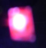
Fig. 4 Picture of the device with mixed coating of CdSe/ZnS NCs and Au NPs. |
![]()
![]()
Professor Zhe-Chuan Feng
Graduate Institute of Photonics and Optoelectronics, National Taiwan University
Reflective second harmonic generation from ZnO thin films
A study on the Zn-O bonding
by K.Y. Lo, Y.J. Huang, J.Y. Huang, Z.C. Feng, W.E. Fenwick, M. Pan and I.T. Ferguson
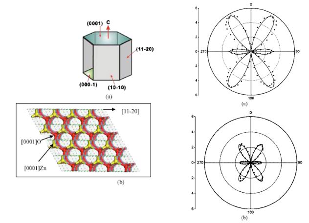
The structures of the Zn–O bonding in ZnO (0002) thin films prepared by metal organic chemical vapor deposition (MOCVD) have been studied by reflective second harmonic generation (RSHG). The polar Zn–O bond on the top layer is not canceled out and presents 3 mm symmetrical structures on the well-grown ZnO (0002) surface. The average polar strength of the Zn–O bond is correlated with the quality of the ZnO (0002) thin film. The mirror symmetry is caused by the nonvanished polar of twin boundary due to the mismatch between the ZnO film and sapphire substrate and analyzed using s-polarized RSHG with s-polarized fundamental light irradiation. These results demonstrate that the Zn–O heteropolar bonds on the smooth ZnO surface contribute to the SHG intensity.
APPLIED PHYSICS LETTERS 90, 161904 (2007)
|
|
|
|
FIG. 1. (a) Hexagonal wurtzite crystal structure of ZnO (0002); (b) symmetrical structure of Zn–O bonding on the surface of ZnO (0002). |
FIG. 2. RSHG patterns from two ZnO films of (a) sample A and (b) sample B. Theoretical fits of the SS-RSHG experimental patterns are drawn in solid line. |
![]()
![]()
Synthesis of photonic crystal slab line-defect waveguides
Professor Yean-Woei Kiang’s Group
Graduate Institute of Photonics and Optoelectronics, National Taiwan University
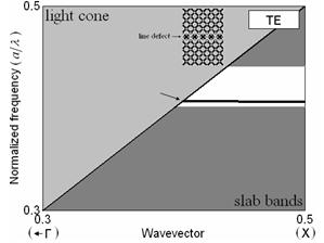
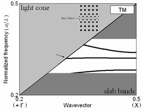
A photonic crystal generally consists of two or more materials with different dielectric constants. These different materials are arranged periodically with a period on a length scale of optical wavelength. Analogous to semiconductor crystals, the periodic refractive index of photonic crystals can cause the destructive or constructive interference. This provides some ranges of frequency called photonic band gaps in which light cannot propagate in the crystal. With photonic crystals, one can manipulate the optical wave in a wavelength scale, leading to many applications such as waveguides, micro-cavities, filters, etc. If a line defect is properly introduced in a photonic crystal slab, one can obtain a photonic crystal slab line-defect waveguide with certain desired spectral property. In other words, it is possible to manipulate the band structure or dispersion relation of the waveguide by properly designing the spatial structure of the photonic crystal. For example, flattening the dispersion relation of some wave mode can result in the reduction of group velocity. This may lead to the realization of slow light with the application of delay devices. This kind of research can be formulated as an inverse problem for synthesizing a photonic crystal structure subject to some specific conditions of band diagram. In this research, the simulated annealing algorithms together with the plane wave expansion method and the effective index method are used to synthesize the photonic crystal slab line-defect waveguides with various values of group velocity.
|
|
|
|
Fig. 1 Band diagram of synthesized photonic crystal slab line-defect waveguide. The band marked by an arrow represents the TE line-defect mode. The average group velocity is 0.0194c. |
Fig. 2 Band diagram of synthesized photonic crystal slab line-defect waveguide. The band marked by an arrow represents the TM line-defect mode. The average group velocity is 0.0212c. |
|
Wide Band Gap Semiconductor Lab. |
We mainly focus on the investigation and applications of wide band gap semiconductors of SiC, ZnO, GaN and related materials as well as their micro- and nano-structures/devices.
Innovative investigation on bulk and epitaxy SiC materials for power and micro-electronics application and development
 Silicon
carbide (SiC) is an attractive material for applications in high power and
high temperature devices and energy-saving electronic systems. SiC is
currently recognizing as “the energy-saving power semiconductors for the 21st
century” and will play a key important rule in the economic development of
recent decades. R&D in SiC has been greatly revitalized in recent two
decades, especially in recent years in the world range although it has
slackened previously because of the difficulties in growing large size SiC
crystal and the advances in Si technology/industry. SiC polytypes are
promising materials for advanced electronic devices working at high
temperature, high power, high frequency and high radiation environments with
energy less consummation. SiC has a potential to combine the SiC power
electronic devices with the Si-IC technology to open a new era for
energy-saving electronics. But, unlike the cases of Si-based IC, GaN- and
III-V based LED, for which Taiwan R&D and industry production have occupied
important shares in the world range, R&D and industry production on SiC are
very weak in Taiwan.
Silicon
carbide (SiC) is an attractive material for applications in high power and
high temperature devices and energy-saving electronic systems. SiC is
currently recognizing as “the energy-saving power semiconductors for the 21st
century” and will play a key important rule in the economic development of
recent decades. R&D in SiC has been greatly revitalized in recent two
decades, especially in recent years in the world range although it has
slackened previously because of the difficulties in growing large size SiC
crystal and the advances in Si technology/industry. SiC polytypes are
promising materials for advanced electronic devices working at high
temperature, high power, high frequency and high radiation environments with
energy less consummation. SiC has a potential to combine the SiC power
electronic devices with the Si-IC technology to open a new era for
energy-saving electronics. But, unlike the cases of Si-based IC, GaN- and
III-V based LED, for which Taiwan R&D and industry production have occupied
important shares in the world range, R&D and industry production on SiC are
very weak in Taiwan.
|
|
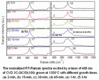
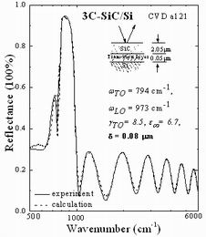
IR reflectance spectrum and theoretical fits, including an interfacial layer, of a CVD-grown 3C-SiC/Si |
Investigation of high efficiency silicon-based thin film solar cells
The highly developments in world culture and economy have leaded to the rapid usage of the earth energy sources, which might destroy the future of human being. Various countries in the world are keenly proposing various plans to open new energy sources for use, to help the sustainable developments for human being. It’s well-known that Taiwan is a country of lacking of energy sources very much. It’s a very important target to develop new energy sources. Solar cells could be one of the most important and very effective ways.
We plan to investigate and develop new types of Si-based thin-film solar cells to serve for Taiwan and the world. In past two-three decades, single crystalline Si solar cells have dominated the market for solar energy application. Thin-film silicon solar cells are expected to become a major type of solar cells, because both the production cost and amount of silicon material used can be reduced in comparison with bulk-type solar cells. This research project proposes to investigate and develop high efficient silicon-based thin film solar cells.
GaN-based Materials and Blue Light LEDs
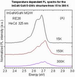
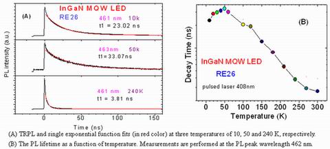
We focus on the investigation of Metalorganic Chemical Vapor Deposition (MOCVD) growth related defects/luminescence engineering, to study the growth associated defects and problems, to penetrate the physical understanding on luminescence mechanism, to find the way to control the defects during the growth procedure and to enhance the luminescence characteristics, and to achieve the high quality of III-Nitrides epitaxial materials. The interdisciplinary investigation via multiple techniques is emphasized.
 |
 |
 |
 |
 |
|
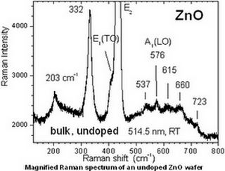
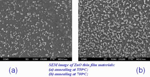
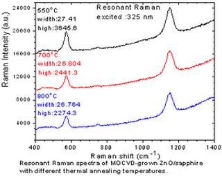
ZnO and Related Materials
In addition, other semiconductors, such as ZnO and III-V InAlGaP, are also included. ZnO is now recognized as the next generation material for lighting industry. In the industry market, InAlGaP and AlGaAs materials are also occupying important share in the semiconductor LED and LD fields, in particular in the red to near infrared spectral range light emitting devices. These red LEDs combining with GaN-based blue-green LEDs can form the entire spectral range white light LEDs. Therefore, we include some investigation on these InAlGaP and AlGaAs hetero-structural epitaxy materials grown from MOCVD technology.
|
|
|
|
|
|
|
|
 |
Please send comments to GIPO_5@cc.ee.ntu.edu.tw.
Copyright
Graduate Institute of Photonics and Optoelectronics, National Taiwan University