|
|
 |
|
 |
| |
Publisher: Chairman Jian-Jang Huang Editors: Professor
Snow H. Tseng, Ms. Hsiao-wen Lin September 30, 2021 |
| |
|
 |
|
Congratulations to Prof. Chee-Wee Liu for being awarded “Pan Wen Yuan Foundation Outstanding Research Award 2021.”
Congratulations to Prof. Chih-I Wu and Dr. Ang-Sheng
Chou for the publication on
Nature
on May 14.
Article on NTU Spotlight:
https://www.ntu.edu.tw/english/spotlight/2021/1949_20210514.html
Article link on Nature:
https://www.nature.com/articles/s41586-021-03472-9
Congratulations to Prof. Yuh-Renn Wu and Prof. Chao-Hsin Wu for achieving Second Place in the “NTU Faculty Combined Badminton Competition 2021.”
|
|
 |
|
 |
|
| |
|
|
|
March
“GIPO Colloquium” Highlights |
|
|
2:20 pm,
March
12 (Fri.), 2021 |
|
Speaker: |
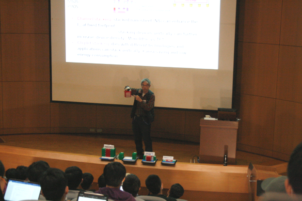
Prof. Chee-Wee Liu (GIPO, NTU) |
|
Topic: |
3Dx3Dx3D: Moore's Law continuing |
|
|
|
 |
|
Prof. Chee-Wee
Liu, Distinguished Professor of
GIPO, NTU |
|
|
|
2:20 pm,
March
19 (Fri.), 2021 |
|
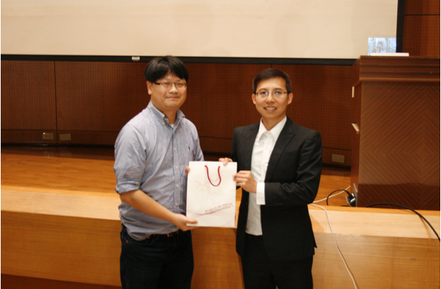
Speaker: |
Lynch Wu (Advanced R&D Division Deputy Director, PlayNitride) |
|
Topic: |
PlayNitride MicroLED Display - PixeLED® Display Technology |
|
|
|
 |
|
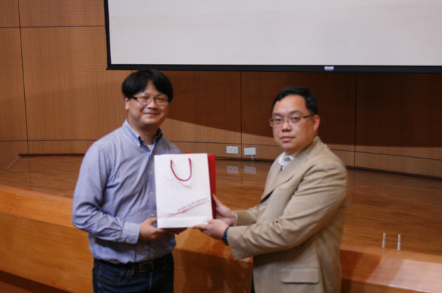
Left: Prof. Hsiang-Chieh Lee. Right: Lynch Wu, PlayNitride. |
|
|
|
2:20
pm, March 26 (Fri.), 2021 |
|
Speaker: |
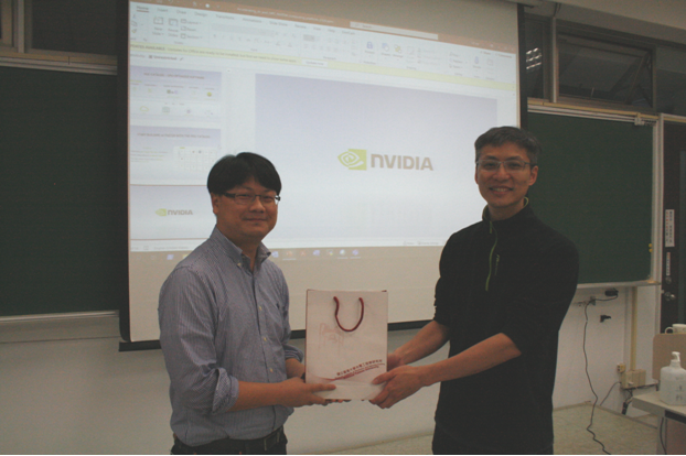
Dr. Cheng-Kuang Lee (NVIDIA AI Technology Center) |
|
Topic: |
Accelerating AI and HPC – NVIDIA computing platform |
|
|
|
 |
|
Left: Prof. Hsiang-Chieh Lee. Right: Dr. Cheng-Kuang Lee,
NVIDIA AI Technology Center. |
|
|
April
“GIPO Colloquium” Highlights |
|
|
2:20 pm,
April 16 (Fri.), 2021 |
|
Speaker: |
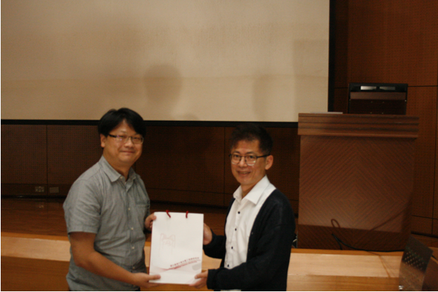
Dr. Mao-Jie Hsu (Tech Director, LuxNet Corp.) |
|
Topic: |
Trends in Semiconductor Laser in Optical Communication Applications |
|
|
|
 |
|
Left: Prof. Hsiang-Chieh Lee. Right: Dr. Mao-Jie Hsu, LuxNet Corp. |
|
|
|
2:20 pm, April 23
(Fri.), 2021 |
|
Speaker: |
Dr. Chen-Hung Lin
(Qisda) |
|
Topic: |
Science/Art & Design/Optimization - An amazing adventure that began with optics |
|
|
|
 |
|
Left: Prof. Hsiang-Chieh Lee. Right: Dr. Chen-Hung Lin, Qisda. |
|
|
May
“GIPO Colloquium” Highlights |
|
|
2:20
pm, May 7 (Fri.), 2021 |
|
Speaker: |
Prof. Ching-Cherng Sun (Department of Optics and Photonics, National Central University) |
|
Topic: |
Optics - New Vision |
|
|
|
 |
|
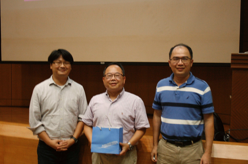
From left to right, Prof. Hsiang-Chieh Lee, Prof. Ching-Cherng Sun, and Prof. Jian-Jang Huang. |
|
|
※ In
response to the growing pandemic,
all further conferences and talks
will be held online. |
|
|
|
|
2:20
pm, May 14 (Fri.), 2021 |
|
Speaker: |
Fu-Ji Tsai (Chief executive
officer, SiriuXense) |
|
Topic: |
From Semiconductor to Optics to Medicine to Smart Care |
|
|
|
June
“GIPO Colloquium” Highlights |
|
|
2:20
pm, June 11 (Fri.), 2021 |
|
Speaker: |
Yih-Jun Won (Deputy Director, Raydium) |
|
Topic: |
Raydium - The Future |
|
|
|
|
|
| |
|
|
|
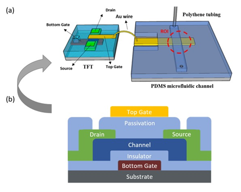
Characterizations of Protein-Ligand Reaction Kinetics by Transistor-Microfluidic Integrated Sensors
Professor Jian-Jang Huang’s Lab
Graduate
Institute of Photonics and
Optoelectronics, National Taiwan
University
Understanding the binding affinities and kinetics of protein-ligand interactions using a label-free method is crucial for identifying therapeutic candidates in clinical diagnostics and drug development. In this work, the IGZO-TFT (thin-film transistor) biosensor integrated with a tailored microfluidic chip was developed to explore binding kinetics of protein-ligand biochemical interactions in the real-time manner. The IGZO-TFT sensor extracts the binding characteristics through sensing biomolecules by their electrical charges. Using lysozyme and tri-N-acetyl-D-glucosamine (NAG3) as an example, we established a procedure to obtain the parameters, such as the dissociation constant, Kd, and association rate constant, ka, that are critical to biochemical reactions. The correlation between the lysozyme concentration and TFT drain current signal was first constructed. Next, solutions of lysozyme and NAG3 of different mixing ratios were prepared. They were pre-mixed for various periods of reaction time before applying to the TFT sensor to extract signals of lysozyme molecules and the concentration remaining. With the knowledge of drain current changes at different reaction times, ka and Kd can be obtained. The values from our experiment are comparable to other methods, which suggests the proposed approach can be employed to explore protein-ligand interaction kinetics in the massively parallel manner if the TFT array is considered.
|
|
|
Fig. 1. (a) Schematic diagram of the IGZO-TFT biosensor integrated with a microfluidic channel. (b) Cross sectional view of the staggered and double-gated TFT. |
|
|
|
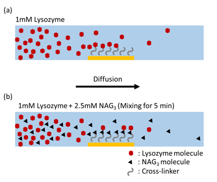
Fig. 2 Illustration of molecule capture process of (a) Lysozyme solution (b) lysozyme + NAG3 solution. Note that in addition to the screening effect, with the presence of NAG3, the drain current will be increased instead of decreased as opposed to the case of purelysozyme solution. |
Flexible
Complementary Oxide Thin-Film
Transistor-Based Inverter with High Gain
Professor
I-Chun Cheng
Graduate
Institute of Photonics and
Optoelectronics, National Taiwan
University
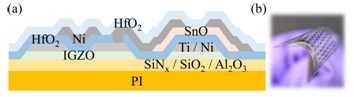
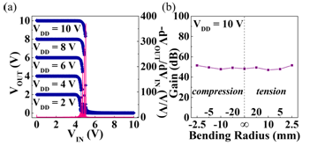
Wearable bio-sensing devices are considered promising for ubiquitous heath monitoring. To accurately read out small bio-signals, the development of high-performance flexible front-end circuits is crucial. Oxide semiconductors are considered one of the most promising active channel materials for on-polymeric-foil electronics. So far, most flexible complementary TFT inverters have been based on either pseudo-CMOS or organic-inorganic hybrid-CMOS configurations. In this study, a high-gain flexible CMOS inverter with a beta ratio (width-to-length ratio between the pull-up and pull-down transistors) of 1 was demonstrated by monolithically integrating a top-gated n-type IGZO TFT and a bottom-gated p-type SnO TFT on a 5.5-μm-thick polyimide substrate, as shown in Figure 1. The IGZO TFT exhibits a field-effect mobility of 8.0 cm2V-1s-1, threshold voltage of 5.2 V, subthreshold swing of 0.15 V/decade, and high on/off current ratio of >107. The corresponding values for the SnO TFT are 1.6 cm2V-1s-1, 2.8 V, 2.3 V/decade and >103, respectively. No apparent current crowding is observed in the output characteristics, suggesting that ohmic contacts exist between the source/drain electrodes and the channel layers. The flexible inverter exhibited a high static voltage gain of 370 V/V and balanced noise margins (noise margin high of 4.8 V, noise margin low of 4.7 V) for a supply voltage of 10 V, as shown in Figure 2(a). In addition, as shown in Figure 2(b), the voltage transfer characteristics remained virtually unchanged when the device was subjected to an outward or an inward bending radius of 2.5 mm, indicating the complementary oxide-TFT-based inverter is practical for flexible electronics applications. [IEEE Trans. Electron Devices, vol. 68, No. 3, p. 1070, Mar 2021]
|
|
|
Fig. 1 (a) Schematic cross section of a flexible oxide-TFT-based CMOS inverter. (b) Photograph of flexible CMOS inverters fabricated on an ultrathin polyimide substrate. |
|
|
|
Fig. 2 (a) Voltage transfer characteristics of a flexible CMOS inverter with a beta ratio of 1 at different VDD. (b) Static voltage gain of the flexible CMOS inverter under different bending conditions. |
Enhancement of Surface Reflectivity of Fused Deposition Modeling Parts
Professor Jui-che Tsai
Graduate
Institute of Photonics and
Optoelectronics, National Taiwan
University
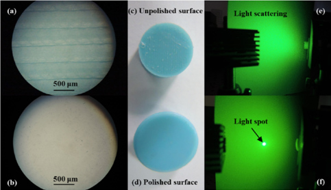
Fused deposition modeling (FDM) parts were enhanced by post-processing to improve surface quality. After reforming with loading and heating applied, the surface can reflect light. Hence, FDM parts with reflective surfaces fabricated from the regular FDM process can be used as optical elements. In printed specimen tests, one surface of the specimen is put on a sheet glass, and both are heated and pressured together to reform the surface of FDM parts. After testing several materials, almost every printed specimen is affected by post-processing, and the optical reflectivity of the FDM parts is increased. However, shrinkage causes a reduced height, and the shape of the FDM parts is deformed dramatically in higher temperature heating condition. The proposed post-processing method improves the surface of FDM parts, and a fabrication process combining this method and investment casting to manufacture optical CCR arrays (possibly with smaller pitches than the original purchased acylic model) was established.
|
|
|
Optical micrographs and light patterns reflected from the surfaces with and without post-processing |
© Elsevier B.V.
Y. F. Chen, Y. H. Wang, and J. C. Tsai, “Enhancement of surface reflectivity of fused deposition modeling parts by post-
processing,”
Optics Communications,
Vol. 430, pp. 479-485, Jan. 2019.
NTU scientists develop giant gauge device of flexible electronics
Professor Yuh-Renn Wu
Graduate Institute of Photonics and
Optoelectronics, National Taiwan University
Professor Wu Yuh-Renn from the Department of Electrical Engineering and Optoelectronics and his Ph.D student Tsai Tsung-Yin, Professor Chang Ching-Ray from the Institute of Applied Physics and the Institute of Electronic Engineering, National Taiwan University and his doctoral student Professor Fuh Huei-Ru (currently teaching at Yuanzhi University), and the Department of Electronic Engineering, Kaohsiung University of Science and Technology Professor Hung Kuan-Ming participated in international team. Recently they developed a method to improve the Gauge factor of strain sensors by using Van der Waals layered materials, which increased the sensitivity by at least 500 times compared with metal materials. By using the mutual interaction of the piezoelectric effect and the photoelectric effect, in addition to the improvement of the Gauge factor, the adjustable range of the Gauge factor is also improved, and it specifically demonstrates its application in the daily activities of the human body to capture small vibration perception. There are important contributions to the principles and applications of learning. The innovative result "Giant Gauge factor of Van der Waals material based strain sensors" was published in Nature Communications on April 1st.
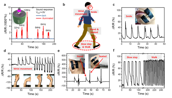
In recent years, software robots, remote monitoring, artificial intelligence, and wearable medical instruments have developed rapidly, and there are higher requirements for the flexibility, sensitivity, and low power consumption of the corresponding sensor. Currently, commercial strain sensors are mainly based on metal materials. However, metal has no energy gap, so the gauge factor of a metal strain sensor is generally limited to a small range of 1-5. Although the energy gap strain of traditional semiconductors is adjustable, traditional semiconductor materials are usually very brittle, which also limits the strain detection range of wearable devices. Compared with metal materials and traditional semiconductor materials, Van der Waals layered semiconductor materials have excellent flexibility, optoelectronic properties and piezoelectric properties, and have huge application prospects in energy storage, optoelectronics, sensing, and wearable devices. Based on this, this cross-international and cross-field team proposed a flexible strain sensor based on Van der Waals layered semiconductor materials. Through the mutual interaction of the piezoelectric effect and the photoelectric effect to adjust the concentration and mobility of carriers, it is the first time that the gauge factor can be continuously adjusted in the range of 23-3933. In addition, as shown in the figure below, the Van der Waals flexible sensor can detect tiny vibrations caused by sound and monitor daily human activities, fully demonstrating its potential applications in robotics, remote monitoring, artificial intelligence, and wearable medical care prospect.
|
|
|
Figure 1: Van der Waals layered material strain sensor is used in the detection of small vibration caused by sound and monitoring of daily human activities. |
Reference:
Wenjie Yan, Huei-Ru Fuh, Yanhui Lv, Ke-Qiu Chen, Tsung-Yin Tsai, Yuh-Renn Wu, Tung-Ho Shieh, Kuan-Ming Hung*, Juncheng Li, Duan Zhang, Cormac Ó Coileáin, Sunil K. Arora, Zhi Wang, Zhaotan Jiang, Ching-Ray Chang, and Han-Chun Wu*,“Giant Gauge factor of Van der Waals material based strain sensors”,
Nat Commun
12, 2018 (2021).
Ultracompact Silicon Waveguide Bends Designed Using a Particle Swarm Optimization Algorithm
Professor Ding-Wei Huang
Graduate
Institute of Photonics and
Optoelectronics, National Taiwan
University
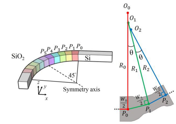
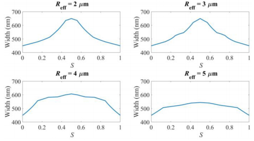
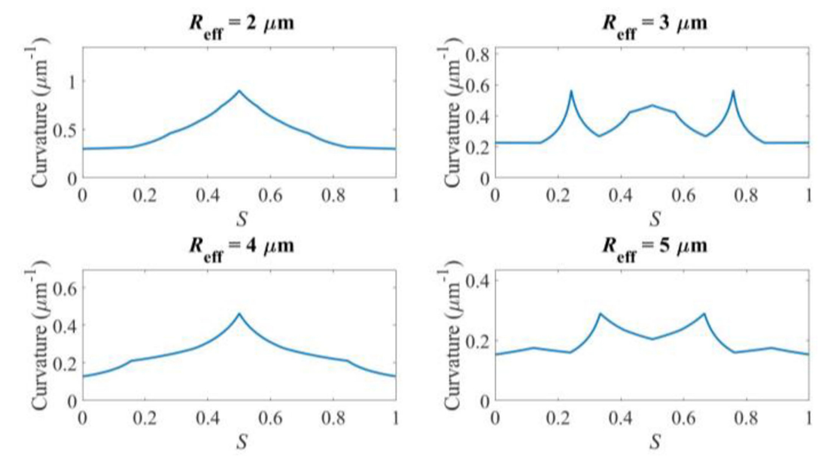
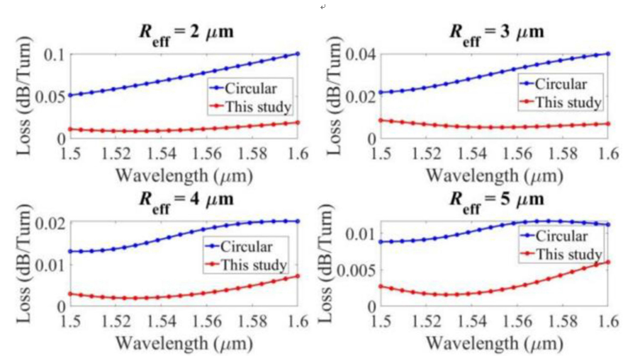
In this study, the trajectory of a 90° bend is divided into two symmetric halves that are mirror images of each other as referenced to the symmetry axis at 45°, and each half is segmented into small curved sections (Fig. 1). The bending radius and waveguide width for every section are parameters to be determined using a particle swarm optimization algorithm. The optimization is performed to maximize the transmission of the waveguide bends, which is calculated by using the three-dimensional finite-difference time-domain technique (Figs. 2 and 3). The results indicate that the total bending loss of the optimized 90° bends with radii of 2, 3, 4, and 5 μm are 0.0106, 0.0051, 0.0025, and 0.0023 dB, respectively, at the wavelength λ = 1550 nm (Fig. 4). In addition, the optimal devices are fabrication tolerant, with fabrication errors in width and height within 10 nm, and less wavelength-dependent compared with circular bends.
|
 |
|
Fig. 1 Schematic for the design method of a waveguide bend. |
|
 |
|
Fig. 2. Width versus length of the normalized light path S of the optimal design. |
|
 |
|
Fig. 3. Curvature versus length of the normalized light path S of the optimal design. |
|
 |
|
Fig. 4. Spectral response of the bending
loss of circular and optimal waveguide
bends for
λ = 1500 – 1600 nm. |
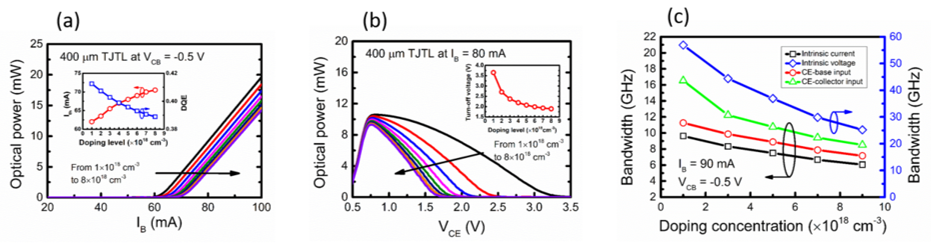
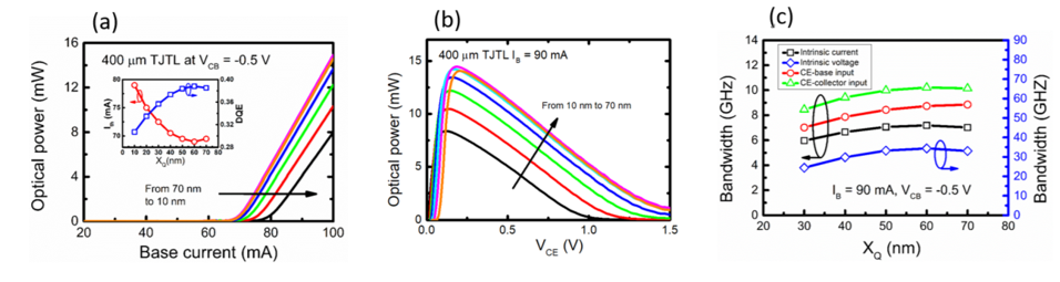
Analytical Modeling of Tunnel-Junction Transistor Lasers
Professor Chao-Hsin Wu
Graduate Institute of Photonics and
Optoelectronics, National Taiwan University
Compared with transistor lasers (TLs), tunnel-junction transistor lasers (TJTLs) are more easily modulated with the voltage across base-collector (BC) junction. In this work, we develop the charge-control model and modified rate equation of TJTLs which includes the Franz-Keldysh effect and direct tunneling. Then, we discuss the effects of the collector-doping concentration and the quantum well position on the performance of TJTL. The capability of the voltage modulation and the optical power are the conflict factors while designing the doping concentration since the heavy doping increases both the junction field and bias-sensitive F-K absorption (Fig. 1(a), Fig. 1(b)). Moreover, the bandwidth decreases when doping concentration increases due to stronger absorption and lower photon density (Fig. 1(c)). For the QW position, we need to find out the optimal position that we can get the best optical confinement to reach the maximum optical output. The result shows that the QW closer to the BC junction can obtain a higher confinement factor to achieve better output power and modulation bandwidth (Fig. 2). Therefore, for the design of TJTLs, the collector-doping concentration and the quantum well position need to be considered to a precise degree to achieve good capability of the voltage modulation with enough output power and bandwidth. [This work has been accepted by IEEE Journal of Selected Topics in Quantum Electronics]
|
 |
|
Fig. 1. (a) The L-I family curves (b) The L-V family curves (c) Bandwidths of the different frequency responses of the TJTL with different doping concentrations. |
|
 |
|
Fig. 2. (a) The L-I family curves (b) The L-V family curves (c) Bandwidths of the different frequency responses of the TJTL with different positions of the QW. |
|
|
|
|
|
|
|
| |
|
|
 |
|
 |
|
|
|