|
August 2019 - October 2019 |
| |
|
|
 |
|
 |
| |
Publisher: Chairman Jian-Jang Huang Editors: Professor
Snow H. Tseng, Ms. Hsiao-wen Lin December 30, 2019 |
| |
|
 |
|
Mr. Shu-Ming Hsu, Doctorate Research Student of Professor I-Chun Cheng, was awarded “European Materials Research Society 2019 Fall Meeting Graduate Student Award”. Congratulations!
|
Award Recipient
|
Advisor |
Thesis Topic |
|
Shu-Ming Hsu |
Prof. I-Chun Cheng |
Complementary Inverters Composed of Oxide Thin-Film Transistors |
Mr. Wei-Li Wu, Master Research Student of
Professor Gong-Ru Lin, was awarded “Chinese Electrical Engineering Society 2019 Best Student Thesis Award Third Place”. Congratulations!
|
Award Recipient
|
Advisor |
Thesis Topic |
|
Wei-Li Wu |
Prof. Gong-Ru Lin |
Pre-compensated frequency division multiplexing algorithms for high-data-rate optical transmission in data centers |
|
|
 |
|
 |
|
| |
|
|
|
~ The
4th International Conference on BioPhotonics;
ICB 2019 ~
(September 15~18, 2019, at Barry Lam Hall, NTU)
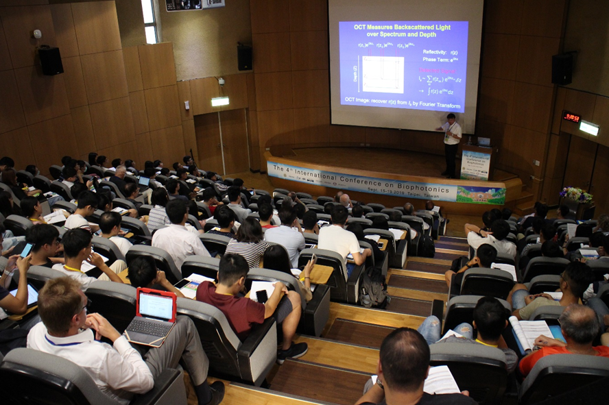
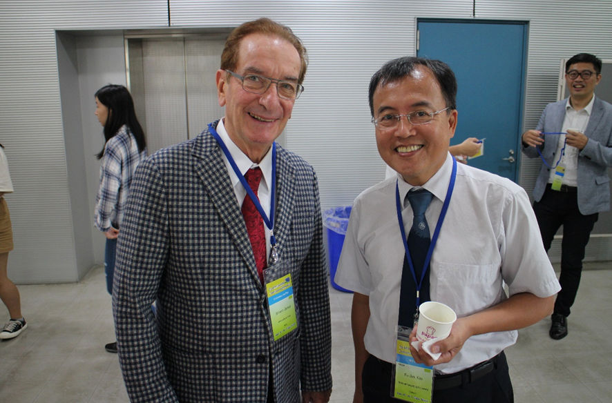
The 4th International Conference on BioPhotonics (ICB; http://icb2019.ntu.edu.tw/) was held at the Barry Lam Hall of the National Taiwan University during Sept. 15–18, 2019. More than 150 scholars and graduate students were registered from more than 10 countries. The goal of the ICB is to have technical exchanges and networking among the leading academics worldwide. Emergent areas that have the potential to significantly benefit our future life, such as precision medicine, cell/immune-therapy, liquid biopsy, optical biopsy, artificial intelligence on biomedicine, were addressed in the 42 papers during the ICB 2019.
Many renowned speakers shared their latest achievements and insights on the future of research in biophotonics ranging from life science to clinical applications. Professor Xingde Li, Johns Hopkins University, U.S.A. addressed OCT and endomicroscopy towards visualization of histology; Prof. Marcus Sauer, University of Wuerzburg, Germany addressed single-molecule sensitive super-resolution microscopy, and Prof. Ann-Shyn Chiang, National Tsing Hua University addressed mapping the Drosophila engram.
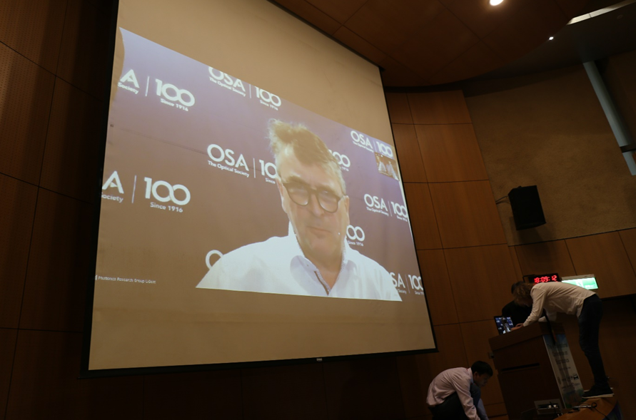
This year, we had a teleconference session, which was delivered by Prof. Roel Baets of the Ghent University, Belgium. He delivered the talk while he was in Washington DC, US. It was a good experience to witness the power of photonics technology by reducing the physical transportation in response to global warming.
The ICB 2019 was jointly sponsored by the National Taiwan University, the Taipei and Italy Chapters of IEEE Photonics Society, IEEE Engineering in Medicine and Biology Society, and Taiwan Photonics Society. The Organizers also appreciate the funding support by the Ministry of Science and Technology, Taiwan as well as the industrial sponsorships from Apollo Medical Optics and Crystalvue Medical Corporation.
|
 |
|
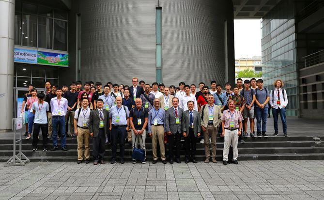
Fig. 1
Group photo of the ICB 2019 participants. |
|
 |
 |
|
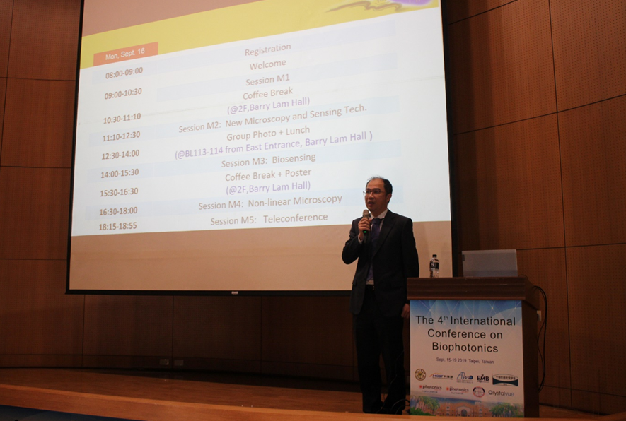
Fig. 2 Welcome address by Prof. JianJang Huang, Chairman, Graduate Institute of Photonics and Optoelectronics, National Taiwan University. |
Fig. 3 Plenary speech by Prof. Xingde Li, Johns Hopkins University, USA. |
|
 |
 |
|
Fig. 4 Teleconference by Prof. Roel Baets, Ghent University, Belgium. |
Fig. 5 The IAC Chair (Prof. Silvano Donati, left) and TPC Chair (Prof. Fu-Jen Kao, right). |
|
 |
 |
|
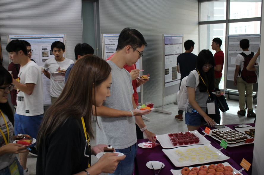
Fig. 6 Lunch time at the Barry Lam Hall. |
Fig. 7 The poster session of ICB 2019. |
|
|
|
|
|
|
| |
|
|
|
Saturated two-photon excitation fluorescence microscopy for the visualization of cerebral neural networks at millimeters deep depth
Professor Chi-Kuang Sun
Graduate Institute of Photonics and
Optoelectronics, National Taiwan University
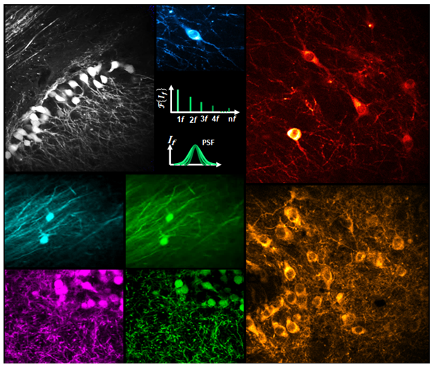
Scattering and absorption of light are inherent barriers in maximizing the imaging depth in biological tissues. To overcome such limitations, fluorescence imaging modalities based on the engineering in the temporal domain has been gaining popularity. The basic mechanism in this domain is based on the repetitive saturated excitation (SAX) of fluorescence. The SAX of fluorescence creates higher nonlinearity, thereby slimmer nano-scale fluorescence point-spread-function (PSF) and higher spatial resolution (Fig. 1). A laser source for excitation is encoded with intensity modulation of a fundamental frequency, and excited fluorescence signal is decoded based on lock-in detection at the modulation frequency. When fluorescence saturation occurs, higher harmonics of the fundamental modulation frequency emerge as a consequence of saturation distortion. Different orders of higher nonlinearity from fluorescence saturation could thus be separated without interference. Therefore, super resolution could be achieved temporally with low vulnerability to optical scattering.
In our study, we have demonstrated the capability and superiority of saturated two-photon excitation fluorescence microscopy (TP-SAX) over the conventional two-photon fluorescence microscopy (TPFM) for the visualization of neuronal networks in an intact transparent (CLARITY treated) mouse brain with transgenic GFP labeling (Fig. 1) at deep depth (Chakraborty et al. J. Biophotonics e201800136, 2018). Here, TP-SAX was achieved with intensity modulated Ti: sapphire femtosecond laser at a fundamental frequency for the two-photon excitation of contrasts. For TP-SAX, a resolution enhancement by a factor of ~ 1.45 times can be observed at 2.4 mm depth of the transparent mouse brain in comparison with TPFM where scattering seriously degraded the PSF. Hence, TP-SAX can be used for exquisite visualization of delicate cerebral neural structure in the scattering regime with a sub-micron spatial resolution inside the intact mouse brain.
|
|
|
Fig.1 Comparison of the imaging performance of TP-SAX, TPFM, and laser scanning confocal microscope (LSCM) in neuronal imaging. Magenta: LSCM image; Green, and Orange hot: TPFM images; Red, Cyan hot, Gray and Cyan: TP-SAX images. (Published as Back cover of the 1/2019 issue of Journal of Biophotonics, DOI: 10.1002/jbio.201800136) |
High Efficiency Laser Phosphor Lighting with Diffractive Optical Elements design for Beam Shaping
Professor Hoang-Yan Lin
Graduate Institute of Photonics and
Optoelectronics, National Taiwan University
The ways for creating an efficient white light source are developed with challenges since several years ago. In solid-state lighting (SSL), laser diodes (LDs) offer a better efficiency at high power density applications compared to other lighting sources, such as, light emitting diode and organic light emitting devices. Therefore, the hot spot on phosphor plate which is produced by laser beam, critically influence the performance of laser phosphor lighting systems. Diffractive optical element (DOE) was introduced to homogenize the optical beam from LDs. Design of a DOE for beam shaping with uniform illumination has been widely employed for several applications, such as, laser cutting, laser drilling, and material ablation, etc.
In such uniform illumination processing, strong zero-order patterns frequently arise owing to the manufacturing error, which drastically reduces the uniformity of the diffraction pattern. Some methods for zero-order suppression have been reported, e.g., adjusting the amplitude and phase profiles by using a spatial light modulator (SLM) and using an off-axis system or additional elements. Estimation of the manufacturing error is indispensable for numerically calculating the phase profile of transmission functions of DOEs. By taking a simulated algorithm of laser beam shaping, the optical properties for the laser phosphor lighting system are improved with a beam shaping DOE.
The method we propose in this paper provides a high-power conversion efficiency for high power density laser lighting system. This approach might be beneficial for enhancing the lifetime and efficiency of the phosphor plate, which are hampered by the thermal issue due to hot spot from laser focusing, and improving the performance of laser phosphor lighting systems.
|
|
|
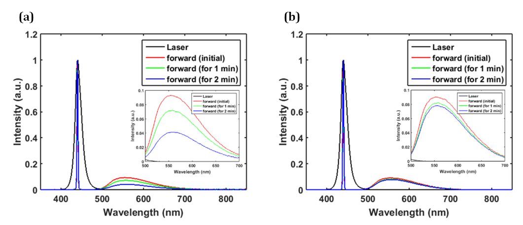
Fig. 1. Radiation spectra of laser phosphor lighting system with laser optical power of 2W (a) without DOE beam shaping (b) with DOE beam shaping. |
Ref. Min-Chian Wu, Yao Lee, Hoang Yan Lin, Chih-Hsuan Tsuei, Chih-Sheng Jao, Kuo-Hsiang Chien, High Efficiency Laser Phosphor Lighting with Diffractive Optical Elements design for Beam Shaping, SID 2019.
|
|
Toward High-Power Blue FPLD/RCLED/μC-LED based Visible Lighting Communications
Professor Gong-Ru Lin’s Laboratory
Graduate Institute of Photonics and
Optoelectronics, National Taiwan University
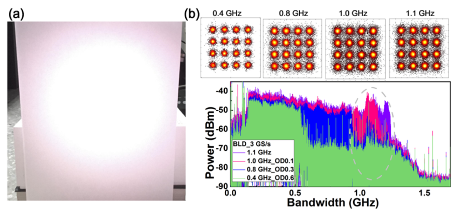
In this research topic, the laser white-lighting at a correlated color temperature (CCT) of 6500K is demonstrated by employing the red/green/blue (R/G/B) tri-color laser diodes (LDs), which introduces the wavelength division multiplexing technology to deliver the 16-QAM OFDM data stream at 11.2 Gbps over a 0.5 m free-space link. In this work, the sampling rate of encoded data is optimized to avoid the aliasing effect and to effectively amplify the signal with high on/off extinction and modulation depth. Proper oversampling can decrease the peak-to-average power ratio of the OFDM data and filter out unwanted noise. There are also six different diffusers used to diverge the white-light mixed by the RGB LD beam. By analyzing the color-casting transmittance, surface roughness, CCT uniformity, divergent angle of the diffuser, and the data transmission capacity, the frosted glass (FG2.8) diffuser with high transmittance diverges the white light with the divergent angle of ±20° and supports the highest data rate of 14 Gbps over 0.5 m , as shown in Fig.1(a). Fig.1(b) illustrates constellation plots and spectra of the RGB LD carried 16-QAM OFDM data with different bandwidths and optical density filters.
|
|
|
Fig. 1. RGB LD (a) generated white light with FG2.8 diffuser and (b) carried 16-QAM OFDM data with different bandwidths and optical density filters. |
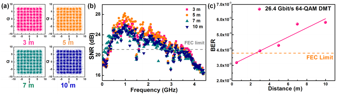
In addition, the violet laser diode (VLD) based ultrahigh-speed free-space optical (FSO) system is demonstrated for point-to-point data transmission. By directly encoding the VLD with the 64-QAM discrete multi-tone (DMT) data stream for the optical wireless communication through 0.5-10 m in free space, the point-to-point VLD-based FSO link allows delivering the 64-QAM DMT data at an ultrahigh bit rate of up to 26.4 Gbps. After receiving with a high-speed p-i-n photodiode, such a VLD-FSO link can provide clear constellation plot with error vector magnitude (EVM) of 8.57%, signal-to-noise ratio (SNR) of 21.34 dB and bit error ratio (BER) of 3.17×10⁻³ under forward-error-correction criterion. The EVM increases from 8.8% to 9.4% and the SNR decreases from 21.1 to 20.6 dB to slightly degrade the reachable data rate from 25.8 to 24 Gbit/s with transmission distance lengthening from 3 to 10 m. Fig. 2 shows constellation plots, SNR responses, and BERs of the VLD carried 64-QAM DMT data with bandwidth of 4.4 GHz at different free-space distances.
|
|
|
Fig. 2.(a) Constellation plots, (b) SNR responses, and (c) BERs of the VLD carried 64-QAM DMT data with bandwidth of 4.4 GHz at different free-space distances. |
A New Analytic Formula for Minority Carrier Decay Length Extraction from Scanning Photocurrent Profiles in Ohmic-Contact Nanowire Devices
Professor Ming-Hua Mao’s
Laboratory
Graduate Institute of Photonics and
Optoelectronics, National Taiwan University
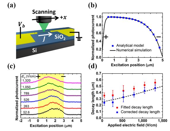
Spatially resolved current measurements such as scanning photocurrent microscopy (SPCM) as shown in Fig. 1(a) have been extensively applied to investigate carrier transport properties in semiconductor nanowires. In this work, we derive an analytic formula for scanning photocurrent profiles in widely used ohmic-contact nanowire devices where the common assumption of carrier diffusion dominance is invalid. Under uniform applied electric fields, weak optical excitation, and the influence of photo-carrier-induced electric field, the scanning photocurrent profile and the carrier spatial distribution strikingly do not share the same functional form. Instead, a surprising new analytic relation between the scanning photocurrent profile and the minority carrier decay length was established. Figure 1(b) shows the calculated scanning photocurrent profiles using analytical model and numerical simulation. The analytic formula is applied in SPCM experiments for an n-InAs nanowire, where electric-field-dependent decay length is found as shown in Fig. 1(c,d).This analytic formula provides a new fitting method for SPCM profiles to correctly determine the minority carrier decay length, which allows us to quantitatively evaluate the performance of nanowire-based devices. This work has been published: Chu, C.-H., Mao, M.-H., Yang, C.-W. and Lin, H.-H.,Scientific Reports
9,
9426, (2019). doi:10.1038/s41598-019-46020-2
|
|
|
Fig. 1. (a) Schematic of a typical SPCM setup. (b) Calculated scanning photocurrent profiles using analytical model and numerical simulation. (c) Measured scanning photocurrent profiles with varied applied electric field. (d) The fitted and corrected hole decay lengths from the measured scanning photocurrent profiles as a function of the applied electric field. |
Development of Anti-UV Structures for OLED Displays
Professor Chung-Chih Wu
Graduate Institute of Photonics and
Optoelectronics, National Taiwan University
Although OLED displays are penetrating into wider applications in consumer electronics due to their high efficiency, high contrast, and good color gamut etc., their extension to outdoor applications (e.g., wearable, vehicular, signage applications etc.) is still facing significant reliability challenges. One major issue is their weak resistance against the UV-light induced degradation; the ultraviolet light (UV-light,
λ<400nm) and high energy visible light (HEV-light, 400 <
λ
< 450 nm) in sunlight would significantly degrade OLEDs and much shorten display lifetimes. Thus, an effective anti-UV technique, that can protect OLEDs from UV/HEV damage and meanwhile maintain display performance, is strongly required. Here we report the development of effective anti-UV/HEV, high-transmittance, high-image-quality structures for OLED display panels based on carefully designed optical thin-film structures composed of more robust inorganic UV-absorbing and dielectric materials, instead of polymer/organic materials that may suffer yellowing by UV radiation.
|
|
|
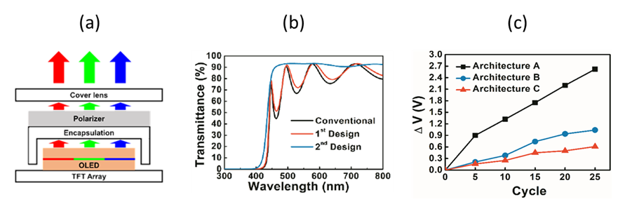
Fig. 1.(a) Typical OLED panel structure. (b) Transmittance spectra of different anti-UV thin film structures. (c) Voltage shifts (ΔV) of test samples under a same current density after repeated solar soaking test cycles. |
|
|
|
|
|
|
|
|
|
| |
|
|
 |
|
 |
|
|
|