|
January 2019 - April 2019 |
| |
|
|
 |
|
 |
| |
Publisher: Chairman Gong-Ru Lin Editors: Professor
Hsiang-Chieh Lee, Ms. Hsiao-wen Lin May 30, 2019 |
| |
|
 |
|
Congratulations to GIPO
Professor Guo-Dung Su on his research paper “One-lens camera using a biologically based artificial compound eye with multiple focal lengths” being published on Optica – a high impact factor SCI journal in optics and optoelectronics.
Article title: One-lens camera using a biologically based artificial compound eye with multiple focal lengths
Website:
https://www.osapublishing.org/optica/abstract.cfm?uri=optica-6-3-326
NTU report website: http://host.cc.ntu.edu.tw/sec/schinfo/epaper/article.asp?num=1387&sn=16898
|
|
 |
|
 |
|
| |
|
|
|
March “GIPO Colloquium” Highlights
(Compiled by Li-Chi Yao) |
|
|
2:20 pm, Mar. 8 (Fri.), 2019 |
|
Speaker: |
Professor Chia-Wei Sun, Department of Photonics, National Chiao Tung University |
|
Topic: |
WIT120
optoelectronics technology |
|
|
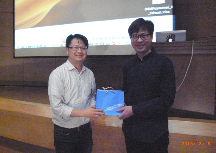
GIPO had the honor of
inviting Professor Chia-Wei Sun to
deliver a speech concerning “WIT120
optoelectronics technology” at
auditorium 101, Barry Lam Hall, on
March 8, Friday. Professor Sun is a
GIPO alumnus and has performed
outstandingly in the academic
circle. His speech was excellent,
rich in content and the professor
interacted very well with students.
GIPO teachers and students
benefitted greatly from this event. |
| |
|
 |
|
Professor Chia-Wei Sun (right) and GIPO
Professor Hsiang-Chieh Lee (left) |
|
|
|
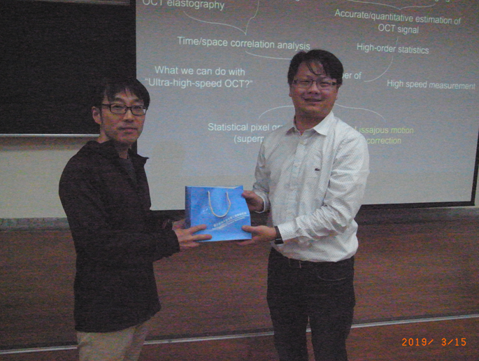
2:20 pm, Mar. 15 (Fri.), 2019 |
|
Speaker: |
Professor Yoshiaki Yasuno, University of Tsukuba, Japan |
|
Topic:
|
1. Signal and image processing of optical coherence tomography
2.
Multi-functional optical coherence
tomography imaging of eye |
|
|
GIPO had the honor of
inviting Professor Yoshiaki Yasuno
to deliver a speech concerning
“Signal and image processing of
optical coherence tomography” and
“Multi-functional optical coherence
tomography imaging of eye” at
auditorium 105, EE Building II, on
March 15, Friday. His speech was
fascinating, and the professor
interacted very well with students.
GIPO teachers and students
participated with enthusiasm and
gained a lot from the event. |
|
|
|
 |
|
Professor Yoshiaki Yasuno (left) and GIPO
Professor Hsiang-Chieh Lee (right) |
|
|
|
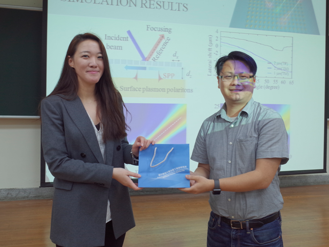
2:20 pm, Mar. 29 (Fri.), 2019 |
|
Speaker: |
Professor Yu-Chieh Cheng, Department of Electro-Optical Engineering, National Taipei University of Technology |
|
Topic: |
Near-field flat focusing mirrors |
|
|
GIPO had the honor of
inviting Professor Yu-Chieh Cheng to
deliver a speech concerning
“Near-field flat focusing mirrors”
at auditorium 105, EE Building II,
on March 29, Friday. Her speech is
marvelous, rich in contents, and the
professor interacted well with
students. GIPO teachers and students
participated in the event with great
enthusiasm and learned a great deal. |
| |
|
 |
|
Professor Yu-Chieh Cheng (left) and GIPO Professor Hsiang-Chieh Lee (right) |
|
|
|
|
|
|
| |
|
|
|
~ 2018 Ph.D. Student Academic Exchange with Nanjing University ~
(The 11th Cross-Strait Ph.D. Student
Forum on Photonic Science and Technology, 2018)
(Time: Nov. 7-11, 2018; Location: National Taiwan University)
Composed by
Jun-Yu Huang,
GIPO Ph.D. student
The Cross-Strait Ph.D. Student Forum on
Photonic Science and Technology is an
important annual academic exchange for
GIPO, NTU, and School of Physics,
Nanjing University (NJU). In 2008, GIPO
Professor C. C. (Chih-Chung) Yang and
academician Shining Zhu,
Nanjing University, achieved a consensus
for establishing the forum, opening up
an over ten-year-long interchange of
academic knowledge and ideas. Moreover,
it is not just a formal exchange, but
also includes several instances of
practical cooperation between the two
universities. This year, there are 15
NJU students and 10 NTU students
representing both sides to participate
in this interflow event.
|
 |
 |
|
NTU Interim President Tei-Wei Kuo addresses the forum. |
GIPO Vice Chairman Jian-Jang Huang hosts the forum’s opening ceremony. |
Generally speaking, this exchange is not
just an academic exchange but also a
wonderful learning opportunity for
participating students. It is different
from conferences or forums that I have
attended before. This exchange is
planned and prepared for thoroughly by
the students of the host university
themselves. Therefore, with NTU as this
year’s host university, students have
learned a lot from its planning and
preparation. Furthermore, we added
something more lively and interactive
into this year’s forum, which is a bit
different from previous years’ forums,
such as raising questions during
meetings and inviting discussions during
poster sessions. All are deliberately
designed to let attendants feel a
greater sense of involvement. During the
forum, both NJU and NTU’s students
performed rather well. NJU student
Xiaohui Tian, in particular, gave
detailed explanations of some novel and
complicate subjects concerning
entangled photon pairs and its
applications, including the fascinating
issue of another possibility of the
quantum computer; therefore, she
obtained NJU’s best paper award. NTU
student Chih-Hao Chuang elaborated on
the recently hot scientific research
topic of 3D AR imaging technique,
including their laboratory’s research
results and the exhibition of their real
product. Eventually, he was also awarded
NTU’s best paper award.
|
 |
 |
|
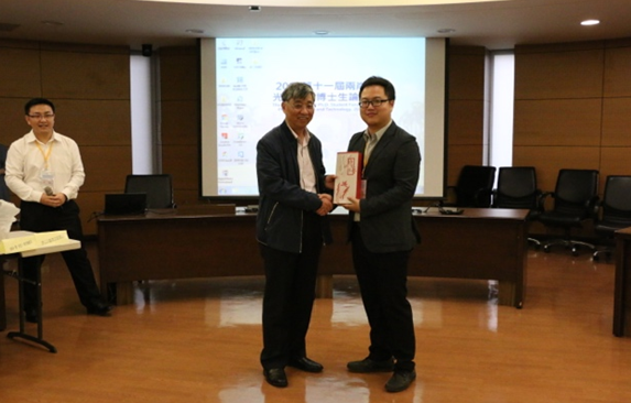
Nanjing University’s best student paper award winner –
Xiaohui Tian |
National Taiwan University’s best student paper award winner –
Chih-Hao Chuang |
It appears that NTU GIPO and NJU School of
Physics’s research fields are quite different.
Due to Taiwan’s industrial structures, NTU’s
research fields tend to be focused on Taiwanese
common industries, such as the manufacturing and
theoretical research involving semiconductors,
optics system design, and light-emitting diodes.
Nevertheless, NJU’s research fields tend to be
focused on physics’ theories, such as the
studies of
entangled photon pairs, biophysics, and
quantum physics, and their research categories
are comparatively extensive. Subsequently, all
participants had the opportunity to discuss and
learn new things with different field’s Ph.D.
students and henceforth stimulate fresh ideas
and unique thinkings.
|
 |
 |
|
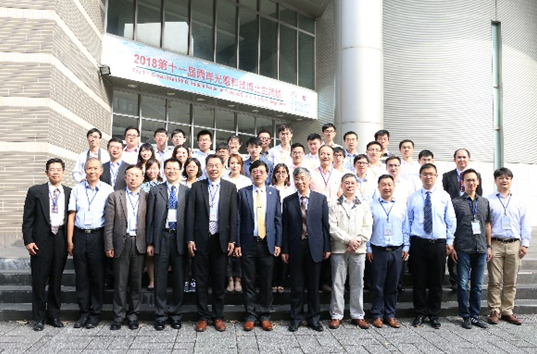
Presented students are attentively listening to the presentation. |
A group photo of all participants |
At the
second day of the forum, at noon, GIPO
Chairman Professor Gong-Ru Lin delivered
a speech concerning the introduction of
Taiwanese snacks, which impressed all of
us greatly. At the same time, we
provided some real Taiwanese snacks for
the far-from-home mainland Chinese
students to enjoy. Having twice the
satisfaction, in mind and in the
stomach, greatly pleased students from
both universities. And finally, this
forum came to an end amid student
laughter and gourmet foods.
|
|
|
|
|
|
| |
|
|
|
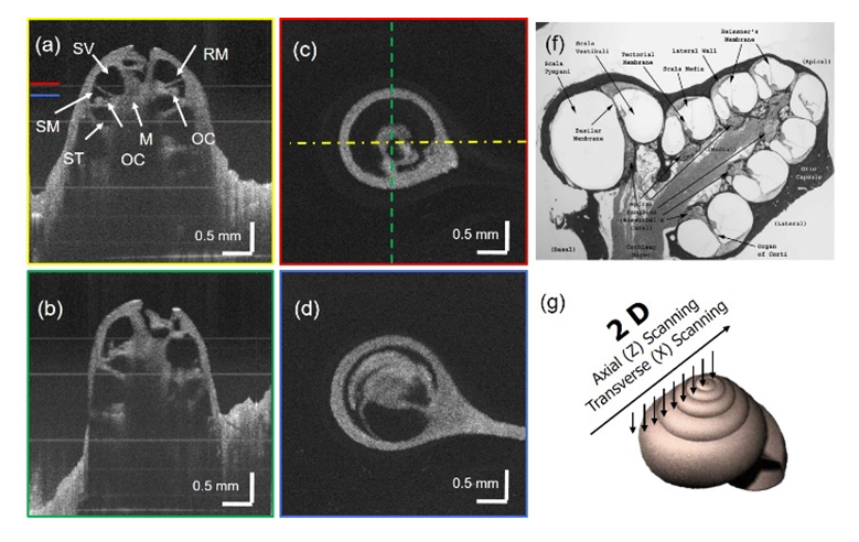
Swept-Source Optical Coherence Tomography Imaging of the Guinea Pig Cochlea
Professor Hsiang-Chieh Lee
Graduate Institute of Photonics and
Optoelectronics, National Taiwan University
OCT is an imaging modality that can be illustrated as the optical analog to ultrasound, where focused light illuminates a sample and backscattered light is collected under use of interferometry. On the other hand, the inner ear is a small and sophisticated organ, mainly comprising the vestibular system and cochlea. In this study, we leverage the technology of swept-source optical coherence tomography to obtain the ex vivo volumetric image of the guinea pig cochlea allowing a better understanding of the cochlear architectures, serving an important step for the subsequent in vivo applications. Moreover, two different center wavelength light sources, i.e. 1.06 µm and 1.3 µm, were used to develop two separate OCT systems, enabling a more detailed investigation on the tissue architectures of the guinea pig cochlea at different regimes as well as different imaging resolutions.
|
|
|
Fig.1 (a) Cross-sectional OCT image of the guinea pig cochlea showed the features with lower OCT scattering intensity reminiscent of the structure in the guinea pig cochlea as shown in (f), the light micrograph of the guinea pig, and inner red line and blue line indicate the position of the en face images (c) and (d), respectively. Yellow and green lines in (c) indicate the position of the cross-sectional images (a) and (b), respectively. Note (f) is reprinted from a previous publication [1]. (M: modiolus; RM: Reissner's membrane, ST: scala tympani; SM: scala media; OC: organ of Corti; SV: scala vestibuli) |
|

|
|
Fig.2 (a) Cross-sectional OCT image of the guinea pig cochlea for 1060 nm SS-OCT system in terms of another transverse scanning direction. (b) for 1030 nm SS-OCT system. |
Reference:
[1] Y. Raphael and R. A. Altschuler, "Structure and innervation of the cochlea," Brain Res Bull, vol. 60, no. 5-6, pp. 397-422, Jun 15 2003.
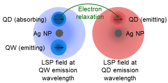
Efficiency enhancement of light color conversion through surface plasmon
coupling
Professor C. C. Yang’s Lab.
Graduate Institute of Photonics and
Optoelectronics, National Taiwan University
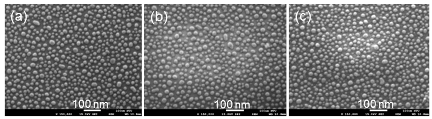
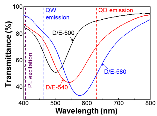
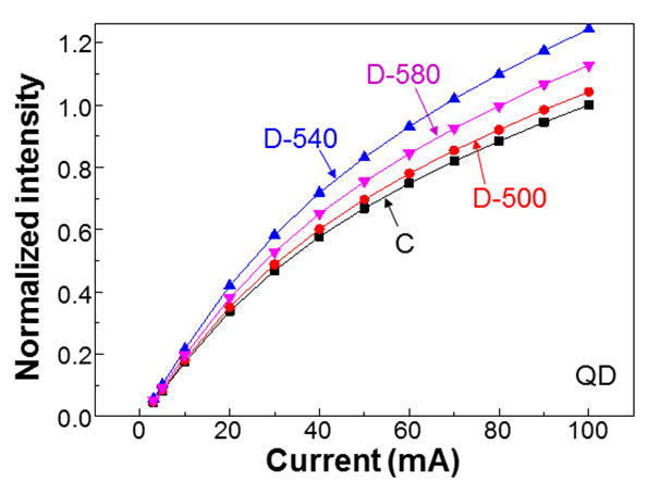
The efficiency enhancement of light color conversion from blue quantum well (QW) emission into red quantum dot (QD) emission through surface plasmon (SP) coupling by coating CdSe/ZnS QDs on the top of an InGaN/GaN QW light-emitting diode (LED) is demonstrated. Ag nanoparticles (NPs) are fabricated within a transparent conductive Ga-doped ZnO interlayer to induce localized surface plasmon (LSP) resonance for simultaneously coupling with the QWs and QDs. Such a coupling process generates three enhancement effects, including QW emission, QD absorption at the QW emission wavelength, and QD emission, leading to an overall enhancement effect of QD emission intensity. An Ag NP geometry for inducing an LSP resonance peak around the middle between the QW and QD emission wavelengths results in the optimized condition for maximizing QD emission enhancement. Internal quantum efficiency and photoluminescence (PL) decay time measurements are performed to show consistent results with LED performance characterizations even though the QD absorption of PL excitation laser may mix with the SP-induced QD absorption enhancement effect in PL measurement. Figure 1 schematically shows the SP coupling mechanism. Figures 2(a)-2(c) show the SEM images of Ag NPs in samples D/E-500, -540, and -580, respectively. Figure 3 shows the transmission spectra of the three Ag NP samples. The transmission depressions correspond to their LSP resonances. A deeper depression at a wavelength indicates stronger LSP resonance. Figure 4 shows the normalized emission intensities as functions of QW injection current in various samples. Among them, the color conversion efficiency of sample D-540 is the highest through LSP coupling.
|
|
|
Fig.1 SP coupling mechanism |
|
|
|
Fig. 2 (a)-(c): SEM images of Ag NPs in samples D/E-500, -540, and - 580, respectively. |
|
|
|
Fig. 3 Transmission spectra showing LSP resonances. |
|
|
|
Fig. 4 Emission intensities of QDs in different samples. |
|
|
Different surface plasmon coupling behaviors of a surface Al nanoparticle between TE and TM polarizations in a deep-UV light-emitting diode
Professor Y. W. Kiang’s Laboratory
Graduate Institute of Photonics and
Optoelectronics, National Taiwan University
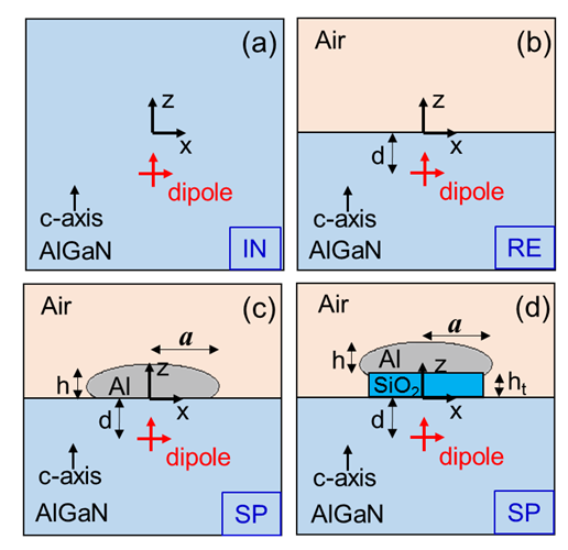
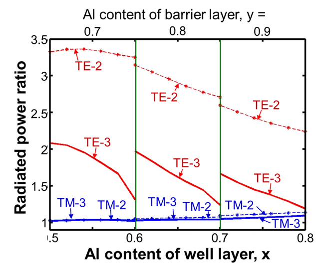
The formulations and numerical algorithms of a three-level model for studying the Purcell effect produced by the scattering of an air/AlGaN interface and the surface plasmon (SP) coupling effect induced by a surface Al nanoparticle in a two-polarization emission system to simulate the transverse-electric- (TE-) and transverse-magnetic- (TM-) polarized emissions in an AlxGa1-xN/AlyGa1-yN (y > x) quantum well (QW) are built. In reasonably selected ranges of Al content for an AlGaN QW to emit deep-ultraviolet (UV) light, the enhancement (suppression) of TE- (TM-) polarized emission is mainly caused by the SP-coupling (interface-scattering) effect. Different from a two two-level model, in the three-level model the TE- and TM-polarized emissions compete for electrons in the shared upper state, which is used for simulating the conduction band, such that either interface-scattering or SP-coupling effect becomes weaker. In a quite large range of emission wavelength, in which the intrinsic emission is dominated by TM polarization, with the interface-scattering and SP-coupling effects, the TE-polarized emission becomes dominant for enhancing the light extraction efficiency of a deep-UV light-emitting diode.
|
|
|
Fig. 1. Four structures for computing the TE- and TM-polarized radiated powers, including the intrinsic (IN) case in (a), the reference (RE) case in (b), the SP-coupling (SP) case without a SiO2 interlayer in (c), and the SP-coupling (SP) case with a SiO2 interlayer in (d). |
|
|
|
Fig. 2. Radiated powers of the TE and TM dipoles normalized with respect to individual levels in the reference case based on either two- or three-level model. The curve of TE-2 (TM-2) corresponds to the ratio of pTE/SP-2 (pTM/SP-2) over pTE/RE-2 (pTM/RE-2). The curve of TE-3 (TM-3) corresponds to the ratio of pTE/SP-3 (pTM/SP-3) over pTE/RE-3 (pTM/RE-3). |
InGaAs photodetector grown on InP substrate with InAsxP1-x metamorphic buffer layers
Professor Hao-Hsiung Lin’s Laboratory
Graduate Institute of Photonics and
Optoelectronics, National Taiwan University
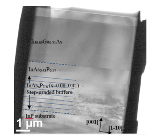
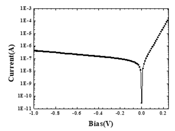
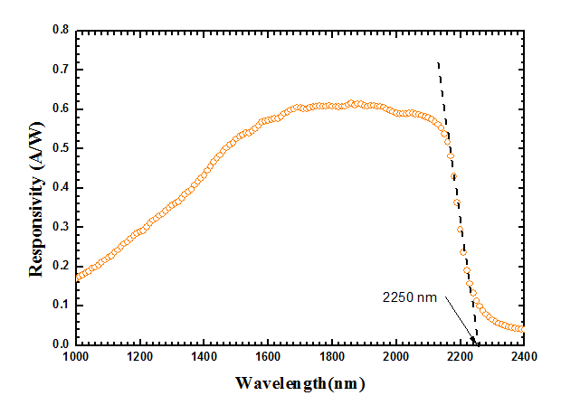
In this work, instead of traditional InAlAs metamorphic buffer, we used step-graded InAsxP1-x layers as the metamorphic buffer for InGaAs/InAsP SWIR photodetectors. InAsP is a mixed group 5 alloy and has the advantages of constant grown rate and low interaction parameter. An In0.69Ga0.31As photodetectors was grown strain-freely on top of the InAsP step-graded layers by MOVPE. Figure 1 show the RSMs for (004) and (115) reflections obtained from the sample, the In0.69Ga0.31As is almost fully relaxed through the using of InAsxP1-x step-graded buffer layers. Figure 2 is a cross-sectional TEM image of the buffer layers showing that misfit dislocations are confined in the buffer layers. No threading dislocation is observed in the In0.69Ga0.31As absorption layer. Figure 3 shows the I-V of a typical metamorphic InGaAs/InAsP detector with a dark current of 4.5×10⁻⁴ A/cm2 at -0.5 V, indicating the good quality of the epilayers. Figure 4 shows the spectral response at zero bias of a detector with a cutoff wavelength of 2.25 µm.
|

|
 |
|
Figure 1. (004) and (115) RSM of InAsP/InGaAs/InAsP/InP structure. |
Figure 2. Cross-sectional TEM image of InAsP/InGaAs/InAsP/InP structure. |
|
|
 |
|
Figure 3. I-V curve of a InGaAs/InAsP detector. Device area is 4×10⁻⁴ cm2. |
Figure 4. Spectral response of a InGaAs/ InAsP detector. |
|
|
|
|
|
|
|
|
|
| |
|
|
 |
|
 |
|
|
|