|
July 2018 - September 2018 |
| |
|
|
 |
|
 |
| |
Publisher: Chairman Gong-Ru Lin Editors: Professor
Hsiang-Chieh Lee, Ms. Hsiao-wen Lin November 30, 2018 |
| |
|
 |
|
Congratulations to GIPO Professor Snow H. Tseng for being elected as the Chair for 2022 Gordon Research Conference (GRC): Lasers in Medicine and Biology (LMB)!
Only the leading experts were invited to the top-notch worldwide biennial conference for lasers in medicine and biology. After three rounds of intense votes, Professor Snow H. Tseng became the first Asian-based researcher voted in as Chair since the conference was established in 1965.
LMB website
A report on the official website of the Electrical Engineering Department of Northwestern University, which is the alma mater of Professor Tseng
An exclusive interview for NTU Facebook
Congratulations to GIPO Professor Snow H. Tseng on being awarded the “Outstanding Life-education Person, 2018” award from the Ministry of Education!
Congratulations! GIPO Distinguished Chair Professor for Research Burn J. Lin is awarded the 2018 Future Science Prize in Mathematics and Computer Science, for pioneering immersion lithography to continuously advance nano-metric integrated circuit fabrication, reviving and extending Moore’s law for multiple generations.
Presenting the Future Science Prize is given in three categories, namely Life Science Prize, Physical Science Prize and Mathematics & Computer Science Prize, with US$ 1 million of award for each. Laureates of the Prize will be selected regardless of their citizenship, as long as their achievements have substantial worldwide effect, are original and innovative, have long-term significance or has passed the test of time, and are completed mainly in the Greater China region.
For related information, please refer to the following links:
http://www.futureprize.org/
https://udn.com/news/story/7240/3356731
|
|
 |
|
 |
|
| |
|
|
|
~ Highlights of the 2018 GIPO undergraduates’ optoelectronics summer camp ~
(Time: August 16-17, 2018; Location: Barry Lam Hall, NTU)
Compiled by
Sheng-Wen Kuo,
the President of GIPO Student
Association
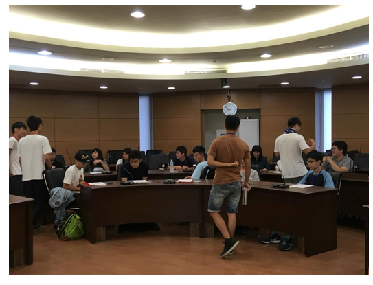
Each summer, GIPO invites undergraduate students from all universities to take part in our optoelectronics summer camp, and this summer was no exception. Participants came from many parts of the country. Some live in Taipei; some live in remote areas. And, we were thrilled to see Pingtung students travel all the way to Taipei to attend our camp. We would, therefore, like to thank you for dedicating part of your vacation time to participate in the GIPO optoelectronics summer camp.
At the start of the event, we divided entire student body into several groups with 6~8 persons per group. Then we spent some time getting to know each student and understanding his or her motivations for participating in this summer camp. Most of their reasons were the desires to know what GIPO students are doing or trying to spend their summer vacation in a more meaningful way. However, there was still another reason that pleased us very much, i.e., they were interested in applying for admission to study at GIPO. And, of course, we were more than delighted to introduce ourselves, and share our daily lives at GIPO, as well as our laboratory experiments.
|
 |
 |
|
Students-counsellor interaction |
Students-counsellor interaction |
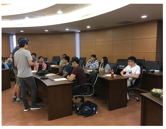
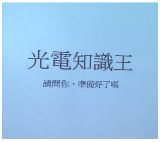
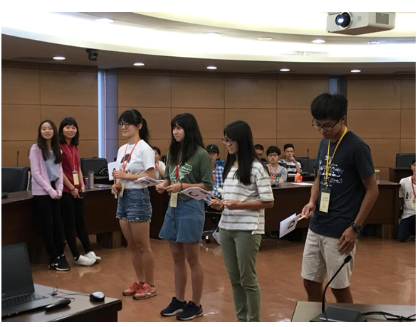
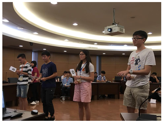
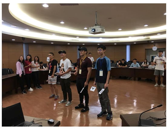
Next, to get to know each other on a deeper level, we set up the “Optoelectronics Knowledge King” challenge, allowing students to interact through competition and accumulate points. Those students with enough points were awarded gifts provided from GIPO. While each student was striving to compete for the honor of his or her group, counselors can observe their behavior, and get to know them better too.
|
 |
 |
|
An "Optoelectronics Knowledge King” projection cover |
A fierce scene of the “Optoelectronics Knowledge King” competition |
|
 |
 |
|
A fierce scene of the “Optoelectronics Knowledge King” competition |
A fierce scene of the “Optoelectronics Knowledge King” competition |
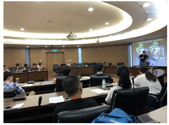
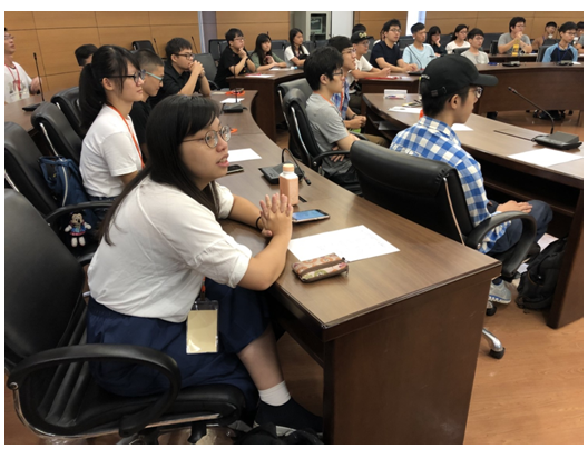
Next, in classroom lessons, we invited GIPO professors and doctoral students to share their optoelectronics-related knowledge with the summer camp students. Students learned some basic knowledge through professors and doctoral students’ professional instruction concerning optoelectronics study and its industrial development. Every student was utterly absorbed in the lessons. Perhaps they are unable to master these lessons instantly; however, they could certainly have gained some studying skills from these experts.
|
 |
 |
|
A
classroom lesson, instructor: Professor Jian-Jang Huang |
Students paying careful attention to the lesson |
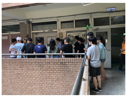
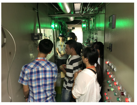
Visiting clean room and E-Beam laboratory was also one of the events to take place during the camp. Although we could not let students operate laboratory instruments, they still developed a deeper impression and basic understanding through a detailed introduction and observing the instruments for themselves. We would like to thank Ms. Fei-Ping Weng, the clean room staff, and Professor Chieh-Hsiung Kuan's laboratory for their help during the visit.
|
 |
 |
|
Visiting the GIPO clean room |
Visiting the E-Beam laboratory |
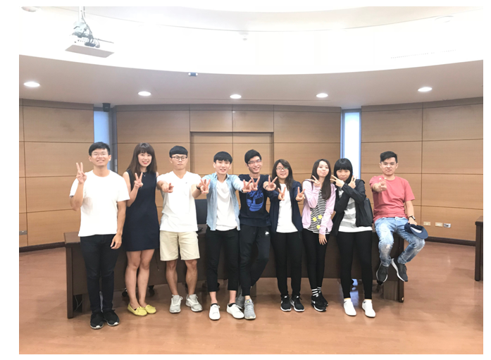
At the end of all activities, certificates were conferred on students who have completed these 2-day courses. Every student was smiling when receiving his or her certificate. We hope they enjoyed attending this camp. And we would like to thank them for participating in this event, which was made worthwhile through their participation. Although it lasted only 2 days, students not only gained a basic understanding of GIPO and optoelectronics but also started to draw up their future plans. After this brief encounter, we are now looking forward to seeing them shine through their talent in the future. Finally, we would like to thank GIPO office staff, professors and students, and our friends at the GIPO student association for their help.
|
|
|
Friends at the GIPO student association |
|
|
|
|
|
|
| |
|
|
|
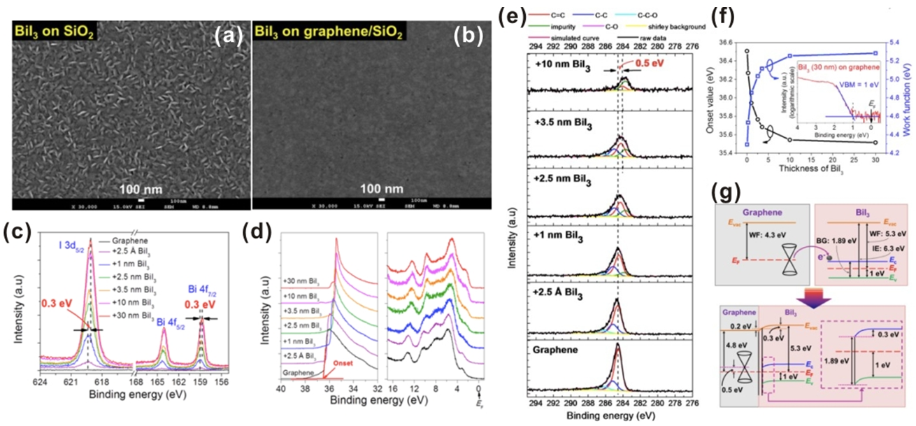
Ultrahigh Responsivity and Superior Sensitivity Graphene-semiconducting Light Absorber Hybrid Phototransistors
Professor Chih-I Wu
Graduate Institute of Photonics and
Optoelectronics, National Taiwan University
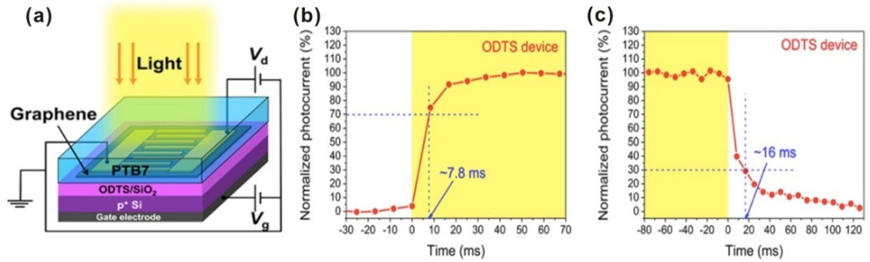
Graphene−semiconducting light absorber hybrid photodetectors have attracted increasing attention because of their ultrahigh photoconductive gain and superior sensitivity. However, most graphene based hybrid photodetectors reported previously have shown a relatively long response time caused by numerous long-lived traps in these hybrid systems, which greatly restricts device speed. In our studies, we found graphene/light-harvesting materials (such as thieno[3,4-b]thiophene/ benzodithiophene polymer (PTB7) and Bismuth(III) iodide (BiI3)) hybrid photodetectors have high responsivity and short photocurrent response time. Figure 1 shows the graphene-PTB7 hybrid photodetectors fabricated on self-assembled-monolayer functionalized SiO2 substrates with a maximum responsivity of ~ 1.8 ×10⁵ A/W and a relatively short photocurrent response time of ~ 7.8 ms.
Besides, the graphene/BiI3 vertical heterostructure phototransistors also have a maximum responsivity of about 6×10⁶ A/W , EQEs of up to 106 % in the visible light region, relatively short photocurrent response times of ~ 8 ms, and detectivity of 7×10¹⁴ Jones under the SNL condition. Compared to BiI3 on bare SiO2 substrates, the thermally evaporated BiI3 films on graphene sheets possessed nearly flatter morphologies and remarkably better crystallinities because of the weak van der Waals interactions between graphene and BiI3. In Figure 2, the photoemission spectra of graphene/BiI3 heterojunctions also manifest the evidence that no chemical interactions occur between graphene and BiI3, resulting in the van der Waals epitaxial growth. The measured band bending consistently illustrates that photo-induced charge transfer occurs at the graphene/BiI3 interface. The high-quality crystal growth of the layered metal halide BiI3 could make graphene/BiI3 heterostructures a promising building block for high-performance optoelectronic applications.
|
|
|
Figure 1. (a) Schematic illustration of a graphene−PTB7 hybrid photodetector (b) Rise time and (c) fall time of the device |
|
|
|
Figure 2. SEM images of 50 nm thermally evaporated BiI3 film on (a) SiO2 and (b) graphene/SiO2. Photoemission spectra of graphene with incrementally increased BiI3 film thickness. (c) XPS spectra of I3d5/2 and Bi4f. (d) UPS spectra for SEC (left) and VB (right) regions, respectively. (e) C1s peak-fitting XPS spectra. (f) The onset values of the SEC spectra (black dot) and the corresponding WFs (blue dot) as a function of the BiI3 thickness. The inset shows the VB maximum position of bulk BiI3. (g) Individual electronic structures of pristine graphene and BiI3. The energy level alignment and band bending at the graphene/BiI3 heterojunction are depicted in the bottom panel. |
Reference :
1. Chang P. H., Tsai Y.C., Shen S. W., Liu S.Y., Huang K. Y., Li C. S. Chang, H. P., and Wu C. I., Highly Sensitive Graphene−Semiconducting Polymer Hybrid Photodetectors with Millisecond Response Time, ACS Photonics 2017, 4, 2335−2344
2. Chang P. H., Li C. S., Fu F. Y, Huang K. Y, Chou A. S., and Wu C. I., Ultrasensitive Photoresponsive Devices Based on Graphene/BiI3 van der Waals Epitaxial Heterostructures, Advanced Functional Materials 2018, 28, 1800179
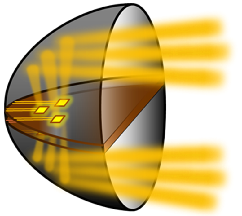
Powerful LED-based train headlight optimized for energy savings
Professor Guo-Dung J. Su's laboratory
Graduate Institute of Photonics and
Optoelectronics, National Taiwan University
A new LED-based train headlight that uses a tenth of the energy required for headlights using conventional light sources has been designed. If operated 8 hours every day, the electricity savings of the new design would reduce emissions of the greenhouse gas carbon dioxide by about 152 kilograms per year.
Train headlights not only illuminate the tracks ahead, they also play an important role in rail transportation. Because trains are difficult to stop, the headlights must be visible from a distance far enough away to give people or vehicles on the tracks ample time to move out of the way. Traditional train headlights, which use incandescent or halogen bulbs, are bright enough to meet safety regulations but are not very energy efficient because most of the energy powering the light is converted into heat rather than visible light.
We were approached by the engineering and design company Lab H2 Inc., to design locomotive headlights that use LEDs as a light source. In addition to requiring less energy, LEDs also last longer and are smaller and more rugged than traditional light sources.
|
|
|
Fig. 1 new train headlight design uses two half-circular parabolic, or cup-shaped, aluminized reflectors with high-efficiency LEDs placed in the plane where the two reflectors come together. Combining the strong beams from each reflector generates the light intensity necessary to meet safety guidelines. Image Credit: Wei-Lun Liang, National Taiwan University. |
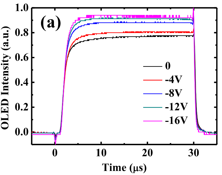
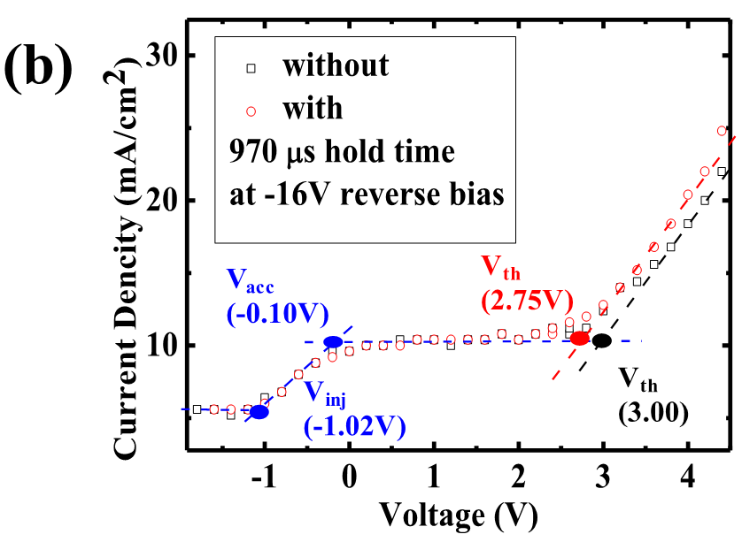
Transient carrier trapping effect in organic light-emitting diode
Professor Jiun-Haw Lee
Graduate Institute of Photonics and
Optoelectronics, National Taiwan University
Transient carrier trapping and de-trapping effect in an organic light-emitting diode (OLED) was studied under different voltage waveforms. As shown in Fig. 1 (a), with 1-kHz voltage pulse at 6 V during on-period of 30 μs and different reverse bias (0 V to -14 V) during the off-period (970 μs), the luminance increased with increasing reverse bias up to 36% due to the trapping effect of positive charge at the cathode and the electron transporting layer (ETL), which was proved by the shift of threshold voltage (Vth) in displacement current measurement with different driving waveforms, as shown in Fig. 1 (b).
|
|
|
Fig. 1. (a) Transient luminance responses with different reverse bias under the off-period. (b) Injection trace from -2 V to 4.5 V of displacement current measurement with different waveforms. |
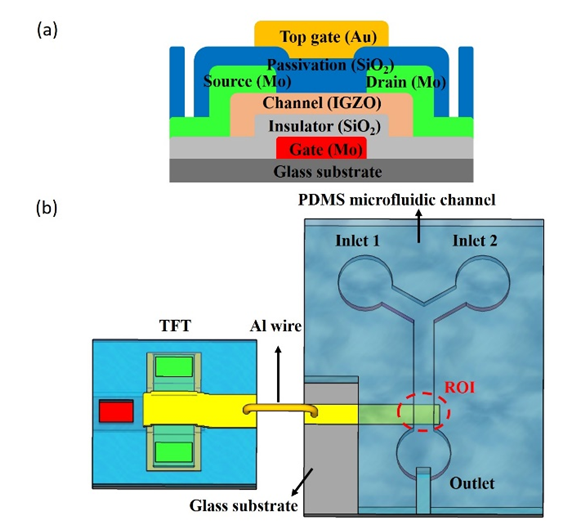
Investigation of Streptavidin-Ligand Biochemical Interactions by IGZO Thin Film Transistors Integrated with Microfluidic Channels
Professor Jian-Jang Huang's laboratory
Graduate Institute of Photonics and
Optoelectronics, National Taiwan University
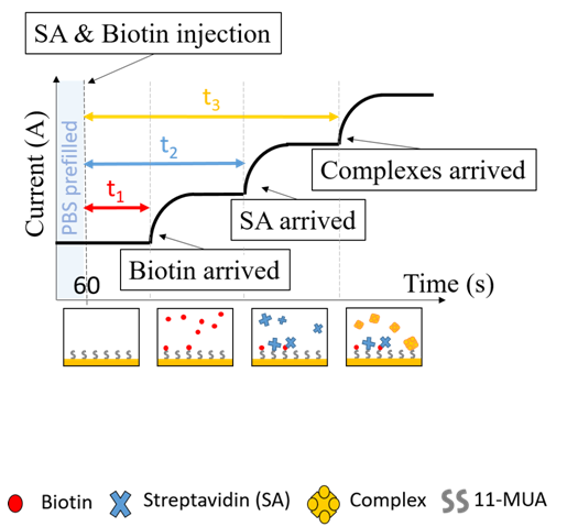
This is a joint research work between Prof. Y.-H. Lo from UCSD and Prof. J.-J. Huang from GIPO NTU. In this work, we demonstrate an IGZO TFT-based biosensor integrated with a microfluidic channel to monitor biochemical reactions between proteins and small molecules. The target biomaterials are applied to a Y-shaped microfluidic chamber while the reactant signal is readout by the TFT. Using Biotin-Streptavidin reaction as an example, the specific diffusion time of biotin, streptavidin, or streptavidin-biotin complex across the fluidic channel are benchmarked. By intentionally delaying the application of one specie to another, one can study properties of biochemical reactions, such as excess and exhaust conditions of the reactants, and the formation of the products while diffusing in the channel. The proposed TFT sensor provides an excellent platform in understanding the biochemical functions for the advance of biological science and drug discovery.
Ref:
This work was published in “Sensors and Actuators B: Chemical. 262.
10.1016/j.snb.2018.01.177”
|
|
|
Figure 1. (a) The cross section of the IGZO-TFT (b) Schematic diagram of a reusable TFT biosensor. The TFT and microfluidic channel were fabricated separately and then connected together by a bond wire. The cross linkers were applied on the surface of ROI. |
|
|
|
Figure 2. Scenarios of drain current responses when the biotin and streptavidin are applied to the fluidic channel. Using the transient response of drain currents, our system is able to detect the complete and incomplete bioreactions. The control measurement was also conducted to verify the reaction between ligands and proteins. |
High-Performance Vertically-Stacked Complementary Inverter Composed of Oxide Thin-Film Transistors
Professor I-Chun Cheng
Graduate Institute of Photonics and
Optoelectronics, National Taiwan University
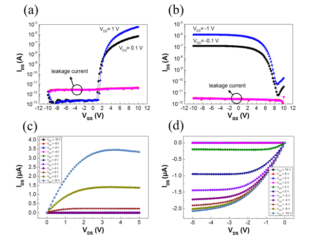
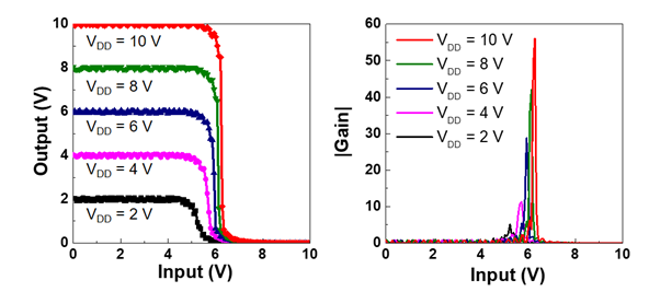
Complementary thin-film transistor (TFT) inverters are the fundamental building blocks for versatile thin-film logic circuits. They possess several desirable features, such as low static power consumption and high density circuit integration. Complementary inverters implemented in a vertically-stacked structure offer an additional advantage, small footprint, in comparison with their coplanar counterparts. Oxide semiconductors are promising candidate channel materials for TFT applications because they have relatively high carrier mobilities and can be processed at low temperatures. In this research, we report an on-glass high-performance vertically-stacked complementary inverter based on oxide TFTs. It is composed of a bottom-gate n-type ZnO TFT stacking on a top-gate p-type SnO TFT. Both active layers were deposited by a low-temperature rf-sputtering technique. Fig. 1 shows the transfer and output characteristics of both the ZnO and SnO TFTs. The ZnO TFT exhibits a threshold voltage of 5.1 V, field-effect mobility of 2.5 cm2/V-s, subthreshold swing of 1.8 V/decade, and on/off current ratio of 2.4х107. The corresponding values for the SnO TFT are 6.2 V, 0.35 cm2/V-s, 0.9 V/decade, and 2.2х104. Fig. 2 shows the static voltage transfer characteristics and gain curves of the vertically-stacked complementary oxide-TFT-based inverter with a geometric aspect ratio of 5 at supplied voltages ranging from 2 to 10 V. A high voltage gain of 56 V/V at a supply voltage of 10 V is achieved. The result demonstrates the feasibility of realizing oxide-TFT based complementary circuits with high-density integration.
|
|
|
Fig. 1 (a)(b) Transfer and (c)(d) output characteristics of the bottom-gate n-channel ZnO TFT and top-gate p-channel SnO TFT. The channel dimensions are W/L = 40 μm/ 20 μm. |
|
|
|
Fig. 2 (a) Static voltage transfer characteristics and (b) gain curves of the vertically-stacked complementary TFT inverter with a geometric aspect ratio of 5 at supply voltages ranging from 2 V to 10 V. |
|
|
|
|
|
|
|
|
| |
|
|
 |
|
 |
|
|
|