|
September 2017 - November 2017 |
| |
|
|
 |
|
 |
| |
Publisher: Chairman Gong-Ru Lin Editors: Professor
Chao-Hsin Wu, Ms. Hsiao-wen Lin January 30, 2018 |
| |
|
 |
|
Congratulations to GIPO professors Gong-Ru Lin on being appointed senior editor, Sheng-Lung Huang and Hoang-Yan Lin on being appointed deputy editors of IEEE Photonics Journal!
Congratulations to GIPO doctoral student Tzu-Chiao Wei on being awarded, under the instruction of
Professor Gong-Ru Lin, “The 1st Doctor Thesis Prize of Lam Research-award, 2017”!
Congratulations to GIPO master student Hao-Lin Yang on being awarded, under the instruction of
Professor I-Chun Cheng, the Best Paper Awards of IDMC (International Display Manufacturing Conference), and IEDMS (International Electron Devices & Materials Symposium 2017)!
Congratulations to GIPO professor Chi-Kuang Sun on being awarded the “61st the Ministry of Education Academic Award
- Engineering & Applying Science”!
Congratulations to GIPO professor Snow H. Tseng on being awarded the “2017 the Ministry of Education Friendly Campus Award
- University/College Excellent Tutors” prize!
Congratulations to the following master student
on being awarded, under the instruction
of Professor Ching-Fuh Lin, the “2017 Youth Thesis Prize of the Chinese Institute of Electrical Engineering
- the 3rd
prize”!
|
Winner |
Advisor
|
Thesis title |
|
Po-Tsun Guo, (master student) |
Ching-Fuh Lin, professor |
Fabrication of Planar Heterojunction Perovskite Solar Cells via Sandwich Deposition Technique |
Congratulations! GIPO professor Chee-Wee Liu receives the title of “2018 IEEE Fellow”.
Congratulations to GIPO doctoral student
Cheng-Ting Tsai on being awarded, under the instruction of
Professor Gong-Ru Lin, the 2017 technology scholarship from CTCI Foundation!
|
|
 |
|
 |
|
| |
|
|
|
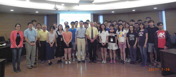
~ Highlights of the 2017 GIPO undergraduates’ optoelectronics summer camp ~ |
|
(July 25-27, 2017 at Barry Lam Hall, NTU) |
|
Compiled by Jui-Hsiang Tsai (the president of GIPO Student Association) and
Chih-Wei Huang (the convener) |
|
Aside
from caring about academic research and
students’ physical and mental health,
GIPO also cares about students who are
interested in joining the Institute.
Therefore, GIPO holds a 3-day-long,
morning until evening, meals,
transportation, and lectures included
wonderful camp each summer, i.e. the NTU
GIPO undergraduates’ optoelectronics
summer camp. This camp is especially
designed for 3rd and 4th year
undergraduate students. Its purpose is
introducing related photonics and
optoelectronics knowledge and GIPO’s
latest developments to prospective
students. The event also provides GIPO
application information to those who are
interested in applying. It is an
excellent opportunity for potential
students to gain some relevant knowledge
before applying for admission.
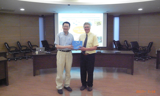
On the
morning of the first day, Chairman Gong-Ru
Lin opened the event by introducing the
general background of photonics and
optoelectronics to students. In the
afternoon, Dr. Chih-Chang Lee, Dr.
Sandeep Chakraborty, Professor Sheng-Lung
Huang and Professor Hsiang-Chieh Lee
separately introduced the technology and
industry of bio photonics, the contents
of which impressed students very much.
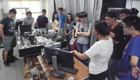
On the morning of the second day, we
visited laboratories. First, we went to
EE1 building to visit its photonics
laboratory. In the laboratory, senior
graduate students showed us the
application of holography, which
combined modern technology with vivid
filming, spurring our desire to study
holography and learn more. After the lab
tours, Professor Jian-Jang Huang
delivered a speech concerning the
technology and industry of solid-state
lighting, and then Professor I-Chun
Cheng delivered another speech
concerning the technology and industry
of solar cells. These two professors’
wonderful speeches benefitted students a
great deal and invited many enthusiastic
questions. And lunch followed a thorough
question and answer session. In the
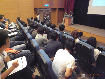
afternoon, IEEE Professor Kent Choquette
delivered a speech concerning “Vertical
Cavity Laser Arrays Present Status and
Future Prospects”, which lasted for 2
hours, but was not boring at all because
students all listened to the speech
attentively. Finally, Dr. Cheng-Ting
Tsai delivered another speech concerning
the technology and industry of
fiber-optic communication, which
concluded the second day’s activities.
The third
day’s activity was visiting relevant
industries. In the morning, we went to
Hsinchu to visit Wistron NeWeb
Corporation. Aside from touring their
facilities, we invited a Wistron
employee, an NTU graduate, to talk about
the job, as well as some job application
skills. In the afternoon, we went to
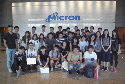
Houli, Taichung, to visit Micron
Technology, Inc. We would like to thank
Micron for providing us with a hearty
meal. After the meal, Micron also
arranged for an employee, also an NTU
graduate, to introduce to us several
things about Micron, which impressed us
greatly. After having visited these
industries, we had a greater
understanding of the future of the
industry and the prospects of photonics
and optoelectronics graduates. Thus,
this 3-day-long camp ended. We would
like to thank all the junior students
for your fervent participation, thank GIPO office staff for their help, and
thank members of the GIPO student
association for your enthusiastic
assistance in the past year. This
association’s 1-year-term will soon be
over, and we will soon hand the post to
a newly elected president; therefore, we
would like to wave farewell to you and
the association, and thank you all for
your kind support in the past year.
~ Self-Introduction of the President of 2017 GIPO Student Association ~
Composed by
Sheng-Wen Kuo, the president of GIPO Student Association
 Hello
GIPO teachers, students and office staff. I am
Sheng-Wen Kuo, the president of the 2017 GIPO
student association. I am honored to be of
service to you in this coming year. Firstly, I
would like to thank Jui-Hsiang Tsai, the former
president of the association, for his
recommendation of me to take over this post and
for his generous help in the handing over of
duties. I would also like to thank the ladies of
the GIPO office for their assistance and advice.
I sincerely hope that I will manage the
association smoothly to extend GIPO’s good
spirits into the next year.
Perhaps some new students are still not
quite familiar with the works of this
association; therefore, I would herewith like to
explain a bit to give everyone a general
understanding. The association is the
representative of GIPO students. It is obligated
to strive for students’ benefit. Furthermore,
the association is also responsible for holding
activities so-as-to create opportunities for
students to get to know each other, and to
increase your friendship circles.
There will be two major events in the following
year. One is the first semester-end party, which
provides delicious foods and splendid
performances for you to enjoy, so as to let
students have a nice afternoon to interact with
each other and leave them with a wonderful
memory of their time in graduate studies.
Moreover, the other is the 2nd semester’s sports
games, which provides an excellent opportunity
for you to meet other students through playing
sports and testing each other’s skills. Of
course, it does not matter whether you win or
lose.
During these two short years, most of us are
either in laboratories doing experiments or
sitting in classrooms listening to lectures.
These two things are indeed very important;
however, this lifestyle can keep you from
getting to know other students and keep you
confined to labs. One of the aims of the student
association is to get you to meet new friends to
improve your relationships with other students
through activities. After having participated in
our activities, you will finally realize that
friendships are quite easy to develop and every
classmate could be a friend. Life is short and
time flies fast. It would be quite a pity not to
have any colorful memories of your graduate
student life. The association is opening its
arms to welcome you. Join us and help expand the
GIPO family. Let everyone’s graduate student
life be not just study but a series of happy
memories.
There are still many areas of the association
that need improvement, and we hope these things
can be achieved through your participation. I am
a new graduate student in Professor Chih-I Wu’s
laboratory. Should you have any suggestion or
fresh idea, please send an e-mail to the
association’s mailbox or drop in to our
laboratory for a chat. We would herewith like to
thank GIPO office staff for your help, and thank
our directing professors for their support.
Finally, we sincerely invite every student, new
or old, to join us to make the association
stronger.
|
|
|
|
|
|
| |
|
|
|
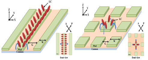
A 3D electrode design for
fast-response VA-FFS liquid crystal mode
Professor Wing-Kit Choi
Graduate Institute of Photonics and
Optoelectronics, National Taiwan University
In this work, a 3D electrode design
is proposed [1] for a Vertically-Aligned Fringe-Field Switching (VA-FFS or Dual-FFS)
liquid crystal mode which is known for its intrinsic sub-millisecond fast
response time without using thin cell gap or other liquid crystal phases.
Compared to the previously proposed 2D electrode designs [2-3], we found that,
by using this new 3D electrode design, it is possible to improve the potential
maximum transmission due to reduced disclination lines or deadzones (without
using a double-sided electrode structure) and also to improve the potential
response speed due to smaller effective domain size of liquid crystals. A major
mechanism for causing such a fast response time is due to the formation of
self-imposed boundaries [3] (or so-called virtual walls) which can be viewed as
liquid crystals having very small “effective” cell gap. This proposed approach
of achieving fast response time in liquid crystals can be very attractive since
it doesn’t require more complicated liquid crystal phases (or materials) such as
Blue Phase or SmC* Ferroelectrics. This approach may simply use standard nematic
liquid crystal phase or materials such as E7. Moreover, this approach doesn’t
require the use of very thin cell gap (e.g. 2μm or below) which is less
practical for large area fabrication. This proposed technique of achieving fast
response time in liquid crystals can therefore be attractive for the future
development of fast response liquid crystal displays, intensity or phase
modulators.
[1]
Wing-Kit Choi, Chia-Hsiang Tung and Bo-Kai
Tseng, “Fast Response VA-FFS Liquid Crystal Mode
using 3D electrode design”, SID 2017 Digest,
pp.1838-1840, May 2017
[2] M. Jiao, Z. Ge, S. T. Wu, and W. K. Choi,
“Sub-millisecond response liquid crystal
modulators using dual field switching in a
vertically aligned cell,” Appl. Phys. Lett., 92,
111101, Mar. 2008
[3] W.K. Choi & S.T. Wu, “Fast response liquid
crystal mode,” US Patent 7298445 B1, Nov. 2007
|
|
|
Fig. 1 shows electrode design and molecular
orientation of 2D VA-FFS (left) and the new
3D VA-FFS (right) at voltage-on state. |
|
|
|
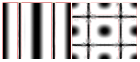
Fig. 2 shows the top-view
transmission of 2D VA-FFS (left) and 3D VA-FFS
(right). The figure on the right shows that
disclination lines (or deadzones) are indeed
reduced along the transverse (or y)
direction in the 3D VA-FFS. |
|
|
|
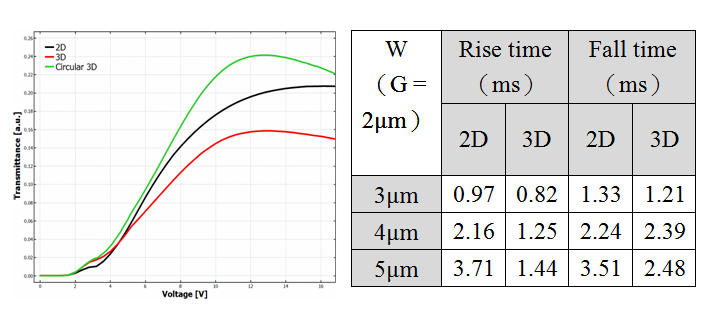
Fig. 3 shows the
improvement of the transmission (figure on
left, with circular polarizer) and also
improvement of response speed (Table on
right) of 3D VA-FFS compared to 2D VA-FFS
liquid crystal mode. |
Threshold Voltage Improvement Through Sidewall
Control of InGaAs Fin-structured High Electron
Mobility Transistors (Fin-HEMTs)
Professor Chao-Hsin Wu’s laboratory
Graduate Institute of Photonics and
Optoelectronics, National Taiwan University
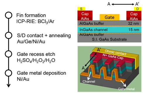
The fabrication process was started
with fin formation by inductively coupled plasma dry etch. The source and drain
metal were deposited by e-beam evaporator and followed by rapid thermal
annealing to form Ohmic contacts. Then, the recess region was etched by diluted
sulfuric acid followed by self-aligned gate metal of Ni/Au. Fin widths were
finally defined by recess etch and varied from 396 to 54 nm. The schematic cross
section and structure are shown in Fig. 1.
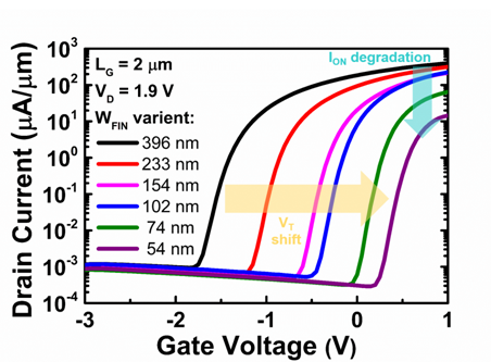
Figure 2 shows ID-VG
characteristics of FinHEMTs with different fin widths (Wfin).
Threshold voltage (VT) shifts toward positive direction from -1.41 V
to 0.56 V as Wfin decreases. It can be observed that compared to
planar devices, VT of Fin-HEMT moves to +VG as Wfin
decreases. As Wfin is reduced down to about 90 nm, the device starts
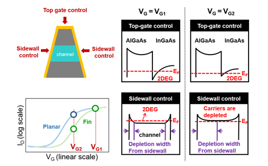
to work at enhancement mode operation. The mechanism is proposed in Fig.3. When
VG decreases from VG1 (large) to VG2 (smaller),
top gate still cannot turn off the channel. So the planar devices are still at
on-state operation. On the other hand, for fin-shaped devices, though top gate
is not capable of turning off the channel, the depletion region from surface of
sidewalls is large enough to fully deplete the channel.
|
|
|
Fig. 1. Process flow, schematic cross
section and device structure of InGaAs Fin-HEMT |
|
|
|
Fig. 2. Transfer characteristics of InGaAs
FinHEMTs with different fin width at VD
= 1.9 V |
|
|
|
Fig. 3. Schematic mechanism of top gate and
sidewall gates proposed in this work |
Multi-Band Infrared Thermal
Emitter with Selectable Polarization
Professor Si-Chen Lee’s laboratory
Graduate Institute of Photonics and
Optoelectronics, National Taiwan University
This study demonstrated a multi-band infrared thermal emitter featuring a narrow
bandwidth emission and polarization characteristics, which is quite suitable to
be applied to the non-dispersive infrared (NDIR) detection system. NDIR system
has been widely used in monitoring the hazardous and harmful substances in the
human living environment. The target molecules can be detected by measuring the
transmission optical energy at specific wavelengths due to their particular
molecular bond vibration, which is inversely proportional to the molecular
concentration in the NDIR system. Because the biomolecules usually exhibit
multiple absorption peaks in the infrared regions, the multi-wavelength infrared
light source plays an indispensable role in the NDIR system. The device is
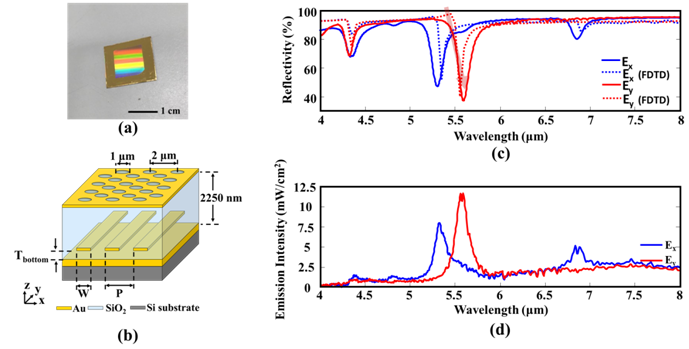
constructed by embedding the metallic grating strips within the resonant cavity
of a metal/dielectric/metal (MDM) structure, as shown in Fig. 1(a) and 1(b).
This arrangement makes it possible to generate waveguide resonances with
mutually orthogonal polarization, thereby providing an additional degree of
freedom to vary the resonant wavelengths and polarizations in the medium
infrared region. The measured reflection spectra and the finite-difference
time-domain simulation indicated that the electric fields of the waveguide modes
with two orthogonal polarizations are distributed in different regions of the
cavity, as shown in Fig. 1(c) and (d). Resonant wavelengths in different
polarizations can be adjusted by altering the period, the metallic line width,
or the position of the embedded gold strips. The ratio of the full width at half
maximum (FWHM) to the peak wavelength was achieved to be smaller than 0.035.
This work has been published in AIP Advances 7,
085122 (2017).
|
|
|
FIG. 1. (a) A photograph of the multi-band
infrared thermal emitter with polarized
waveguide modes. (b) Schematic diagrams of
polarized waveguide thermal emitter. (c) The
experimental and FDTD simulated reflection
spectra in x- and y-polarizations. (d) The
experimental thermal radiation spectra of
the device in x- and y-polarizations. |
High-resolution Analysis of Leaky
Modes in Surface Plasmon Stripe Waveguides
Professor Hung-chun Chang
Graduate Institute of
Photonics and Optoelectronics, National
Taiwan University
The surface plasmon polariton (SPP) existing at
an interface between metal and dielectric
material is a basic phenomenon in the area of
“plasmonics” and has been a well-known wave mode
particularly in the visible and infrared
wavelength ranges. With the rapid progress of
the plasmonics research in recent years, various
SPP waveguides have also been proposed and
investigated. Here, we report our recent studies
of the stripe plasmonic waveguides with a gold
stripe having a silica substrate. Such simple
structure was one of the earlier studied SPP
waveguides. Weeber
et al.
reported
their experimental measurement results of waveguide mode
characteristics of such structure in 2003 [Phys.
Rev. B
68,
115401 (2003)]. Zia
et al.
in 2005 [Phys. Rev. B
71,
165431 (2005)] presented finite-difference
numerical analysis of the same waveguides,
obtained their leaky and bound modes, and
concluded that calculated leaky mode
characteristics could be consistent with the
observed SPP-propagation ones by Weeber
et al.
Zia
et al.
calculated the real and imaginary parts of the
complex effective refractive indices,
neff’s,
of the leaky, quasi-transverse-magnetic
(quasi-TM) SPP modes for different stripe
widths, where
neff
is defined as the modal propagation constant
divided by the free-space wavenumber. We have
recently conducted high-resolution
finite-element numerical analysis of the same
stripe waveguide using an in-house developed
full-vector finite-element imaginary-distance
beam propagation method (FV-FE-ID-BPM) and
discovered some subtle mode-field
characteristics in the leaky modes so that the
neff
versus the stripe width curves appear to be of
non-monotonic variation [H. H. Liu and H. C.
Chang, J. Lightwave Technol.
34,
pp. 2752–2757 (2016)]
|
|
|
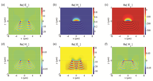
Figure 1 Mode-field profiles of the TM1
mode of the stripe waveguide when the stripe
width is 3.7 μm: (a) Re[Ex],
(b) Re[Hx], (c) Re[Ey],
(d) Re[Hy], (e) Re[Ez],
and (f) Re[Hz]. |
Fig. 1 shows the magnitude profiles of the real
parts of the six field-component phasors of the lowest TM1 mode for
the stripe width of 3.7 μm (the gold stripe thickness is 55 nm). In each panel,
the horizontal thin black line shows the boundary of the substrate, and the
outline of the boundary of the stripe cross-section appears to be the thicker
portion of the thin black line. In the analysis we used 638,347 unknowns for the
computational domain of 8 μm x 11.5 μm size, which covers the right or left half
of the waveguide cross-section making use of the structure symmetry. Such high
spatial resolution and large coverage of the substrate region reveals the
details of the leaky fields in the substrate including the interference feature.
It is interesting to notice that the two stripe edges provide two sources for
the propagating leaky fields. Note that
Hx
(Fig. 1(b)) and
Ey (Fig. 1(c)) are the major
field components. For further discussions, please refer to [J. Lightwave
Technol.
34,
pp. 2752–2757 (2016)].
A method for enhancing the
favored transverse-electric-polarized emission
of an AlGaN deep-ultraviolet quantum well
Professor C. C. Yang’s Lab.
Graduate Institute of Photonics and
Optoelectronics, National Taiwan University
An AlGaN quantum well (QW) structure
of a deep-ultraviolet (UV) light-emitting diode (LED) needs to be well designed
for controlling its band structure such that the heavy-hole (HH) band edge
becomes lower than the split-off (SO) band edge and hence the
transverse-electric (TE) polarization dominates the emission for achieving a
higher light extraction efficiency. Here, we report the discovery of
un-intentionally formed high-Al AlGaN nano-layers right above and below such a
QW and their effects on the QW for changing the relative energy levels of the HH
and SO bands. The comparison between the results of simulation study and
polarization-resolved photoluminescence measurement confirms that the high-Al
layers (HALs) represent the key to the observation of the dominating
TE-polarized emission. By applying a stress onto a sample along its c-axis to
produce a tensile strain in the c-plane for counteracting the HAL effects in
changing the band structure, we can further understand the effectiveness of the
HALs. The formation of the HALs is attributed to the hydrogen back-etching of Ga
atoms during the temperature transition from quantum barrier growth into QW
growth and vice versa. The Al filling in the etched vacancies results in the
formation of an HAL. This discovery brings us with a simple method for enhancing
the favored TE-polarized emission in an AlGaN deep-UV QW LED.
|
|
|
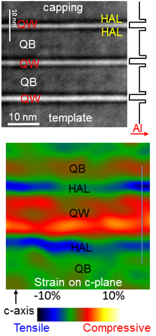
Fig. 1 (upper) TEM image to show the HALs
(dark stripes). (lower) Geometric phase
analysis image.
|
|
|
|
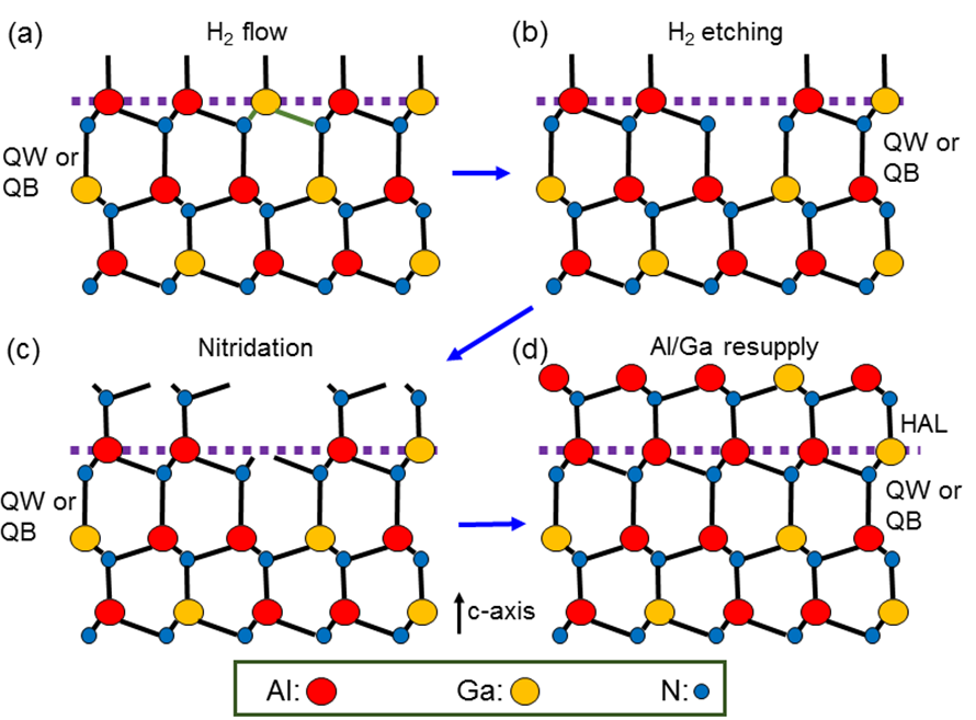
Fig. 2 Schematic drawings to show the
formation mechanism of the HALs. |
Surface plasmon coupling for
suppressing p-GaN absorption and TM-polarized
emission in a deep-UV light-emitting diode
Professor Y. W. Kiang’s laboratory
Graduate Institute of
Photonics and Optoelectronics, National
Taiwan University
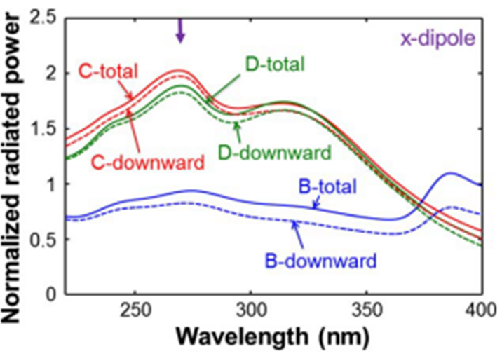
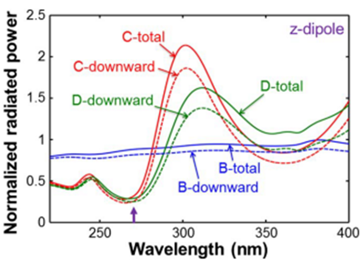
The radiated power enhancement (suppression) of an in- (out-of-) plane-oriented radiating dipole at a desired emission wavelength in the deep-ultraviolet (UV) range when it is coupled with a surface plasmon (SP) resonance mode induced on a nearby Al nanoparticle (NP) is demonstrated. Also, it is found that the enhanced radiated power propagates mainly in the direction from the Al NP toward the dipole. Such SP coupling behaviors can be used for suppressing the transverse-magnetic (TM)-polarized emission, enhancing the transverse-electric (TE)-polarized emission, and reducing the UV absorption of the p-GaN layer in an AlGaN-based deep-UV light-emitting diode by embedding a sphere-like Al NP in its p-AlGaN layer.
|
|
|
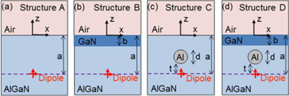
Fig. 1. (a)-(d) Schematic demonstrations of simulation structures A-D. |
|
|
|
Fig. 2. Spectra of the normalized radiated power in structures B-D when an x-dipole is used (d = 50 nm). The vertical arrow marks 270 nm. |
|
|
|
Fig. 3. Similar to Fig. 2 except when a z-dipole is used (d = 50 nm). |
|
|
|
|
|
|
|
| |
|
|
 |
|
 |
|
|
|
|