|
|
 |
|
 |
| |
Publisher: Chairman Gong-Ru Lin Editors: Professor
Chao-Hsin Wu, Ms. Hsiao-wen Lin October 15, 2016 |
| |
|
| |
|
 |
|
April & May “GIPO Colloquium” Highlights
(Compiled by Li-Chi Yao) |
|
|
4:30 pm, April 15 (Fri.), 2016 |
|
Speaker: |
Professor Shiuh Chao (Institute of Photonics Technologies, National Tsing Hua University) |
|
Topic: |
Introduction to Laser Interference Gravitational Waves Detection and the Recent Discovery |
| |
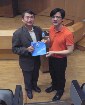
Professor Shiuh Chao visited at the invitation of GIPO professor Sheng-Lung Huang on April 15 (Fri.) and delivered a speech concerning the “Introduction to Laser Interference Gravitational Waves Detection and the Recent Discovery” at auditorium 101, Barry Lam Hall. Professor Chao’s speech was excellent, informative and he interacted very well with students. GIPO teachers and students participated with enthusiasm and learned a great deal. |
|
 |
|
Professor Shiuh Chao (right) and GIPO chairman, Professor Gong-Ru Lin (left) |
|
|
|
4:30 pm, April 22 (Fri.), 2016 |
|
Speaker: |
Dr. Linju Yen
(Investigator & Attending Physician, Institute of Cellular & System Medicine, National Health Research Institutes) |
|
Topic: |
Therapeutic application of human fetal-stage stem cells: differentiation capacity & immunodulatory properties |
| |
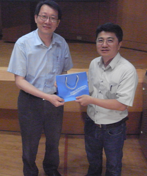
Dr. Linju Yen visited GIPO on April 22 (Fri.) and delivered a speech concerning “Therapeutic application of human fetal-stage stem cells: differentiation capacity & immunodulatory properties” at auditorium 101, Barry Lam Hall. Her speech was fascinating and informative, and she interacted very well with students. GIPO teachers and students attended this event with enthusiasm and learned a great deal. |
|
 |
|
Dr. Linju Yen (right) and GIPO professor Sheng-Lung Huang (left), the host of this speech |
|
|
|
4:30 pm, April 29 (Fri.), 2016 |
|
Speaker: |
Professor Sung-Jan Lin
(Institute of Biomedical Engineering, NTU) |
|
Topic: |
Hair follicle regeneration: How to make something out of nothing |
| |
Professor Sung-Jan Lin visited GIPO on April 29 (Fri.) and delivered a speech concerning the “Hair follicle regeneration: How to make something out of nothing” at auditorium 101, Barry Lam Hall. His speech was wonderful, informative and the professor interacted well with students. GIPO teachers and students took part in this event with enthusiasm and benefitted a great deal. |
|
|
 |
|
Professor Sung-Jan Lin (right) and GIPO professor Sheng-Lung Huang (left), the host of this speech |
|
|
|
4:30 pm, May 6 (Fri.), 2016 |
|
Speaker: |
Professor Tzong-Yow Tsai (Institute of Microelectronics Engineering, National Cheng Kung University) |
|
Topic: |
The technology of Q-switching lasers in all-fiber schemes |
| |
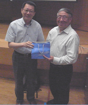
Professor Tzong-Yow Tsai visited GIPO on May 6 (Fri.) and delivered a speech concerning “The technology of Q-switching lasers in all-fiber schemes” at auditorium 101, Barry Lam Hall. His speech was fascinating and the professor interacted very well with students. GIPO teachers and students attended this event with enthusiasm and learned a great deal. |
|
 |
|
Professor Tzong-Yow Tsai (right) and GIPO chairman, Professor Gong-Ru Lin (left) |
|
|
May “Photonics Forum” Lecture Highlights
(Compiled by Li-Chi Yao) |
|
|
10:30 am, May 23 (Mon.), 2016 |
|
Speaker: |
Professor Ji-Kun Chang
(Georgia Institute of Technology, USA) |
|
Topic: |
Fiber Wireless Convergence for 5G Mobile Data Communications |
| |
Professor Ji-Kun Chang visited GIPO on May 23 (Mon.) and delivered a speech concerning “Fiber Wireless Convergence for 5G Mobile Data Communications” at auditorium 101, Barry Lam Hall. His speech was informative and the professor interacted well with students. GIPO teachers and students participated in the event with enthusiasm and learned a great deal. |
 |
|
Professor Ji-Kun Chang (right) and GIPO chairman, Professor Gong-Ru Lin (left) |
|
|
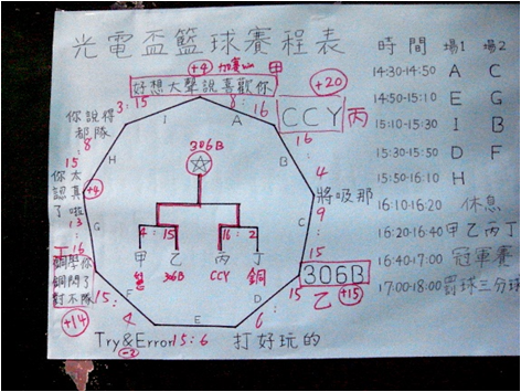
~ Sidelights on the GIPO Cup sports games, 2016 ~
(Time: May 29, 2016; Location: NTUST Gymnasium)
Compiled by
Yu-Ting Huang, the president of GIPO Student Association
GIPO students achieve excellence not only in academic learning, research and behavior, but also in sports as well. Many of them excel in several types of sport. Therefore, GIPO Student Association has decided to hold a ball game to mine your potential and leave you some wonderful memories of your graduate summers for you to share with your children in the years to come.
It was a clear beautiful day, the temperature reached over 30 Celsius. The basketball game and the badminton game were held in the gym of the National Taiwan University of Science and Technology. This gym has no air conditioning, and its basketball court has neither penalty line nor three-point field line. But the super staff of our association resolved these unexpected problems in time, and the games proceeded successfully.
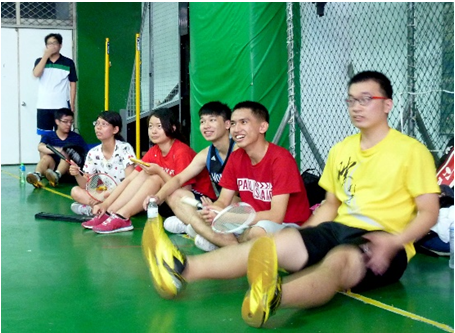
First up was badminton team-play, for which we found several members of the NTU badminton team, hidden within GIPO. The participation of these “super players” made the game extremely intense and exciting. Then, came the badminton singles-play, which was more relaxing and joyful. It looked like the singles’ players were playing the game more for the sake of enjoyment or relaxation than for winning or losing. Finally, the team-play winner came to be the “elder-sister’s right” team. This team won due to their excellent, superior skills. Obviously, everyone should listen to elder-sister Ting-An more often. There was a medal and several cans of badminton birds for each player of the winning team, which should certainly satisfy their constant needs in playing badminton.
|
 |
|
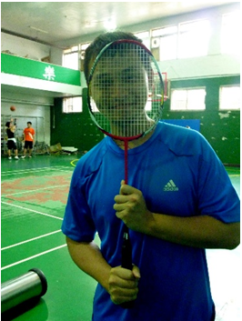
One of the teams competing in the badminton game |
|
 |
|
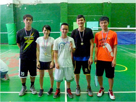
The team that won the badminton championship |
|

|
 |
|
Yi-Jiun Chen, former president of GIPO Student Association |
Kuo-You Huang, a GIPO student who took part in the games |
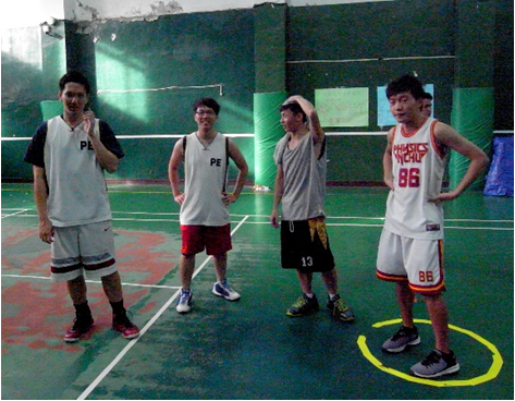
Next, we had the exciting 3-on-3 basketball games. There were 9 teams signed up for this game altogether. During practicing, each team showed courage, willpower, and a determination to win. There was eagerness to win in their eyes, but also expectations to live up to their own standards. Many of them have been playing basketball since their childhood, playing for the team of their department in universities and the team of their institute in graduate schools. Basketball is a passion for them and always will be. To them, basketball is not only a hobby but also precious memories of their youth. So, the GIPO tournament was a special moment, a chance to show the world their remarkable skills and their energy, and their opponents have no escape.
Two hours later, after a series of fierce battles, team “306B” finally won the championship. Players of 306B have excellent skills, seamless cooperative teamwork and unfailing shot accuracy; and they certainly deserved the gold medal. They were each awarded a high-quality basketball for their performance, which will help them continue to hone their skills and get some exercise during their spare time.
|
 |
|
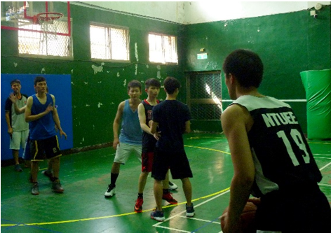
A snapshot of the games |
|
 |
|
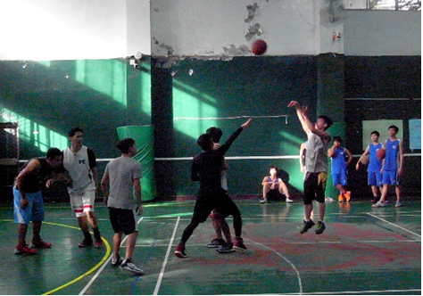
A snapshot of the games |
|
 |
|
The schedule of the games |
|
 |
|
Team 306B, the champions of the 3-on-3 basketball game |
Next, we had the entertaining penalty shot and 3-point shot competitions. In the end, the winner of the penalty shot was Hung-Wen Lin, who also played in the previous 3-on-3 basketball game. At the beginning, in the penalty shot, he threw in all 5 shots and fought into the final. Eventually, Hung-Wen made 9 out of 10 shots at the final and won 1st place. Then, in the 3-point shot competition, he again fought into the final, but lost to upper classmate Chen-Yao Chao by only 1 point. Chen-Yao Chao is truly an outstanding woman, dominating the competition in the 3-on-3 basketball game as well.
Finally, the GIPO games came to a full and satisfying end. We would like to thank the students who came to play, Ms. Yao of GIPO office for her help, and our association members for their constant efforts, from preparations at the beginning to cleaning the site and returning equipment at the end of the games. This was truly a fantastic event, and I am deeply proud of us.
|
|
 |
|
 |
|
| |
|
|
|
Complementary Oxide-TFT-Based Circuits with N-Channel ZnO and P-Channel SnO Thin-Film Transistors
Professor I-Chun Cheng
Graduate Institute of Photonics and
Optoelectronics, National Taiwan
University
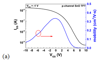
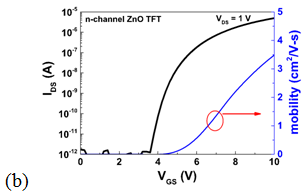
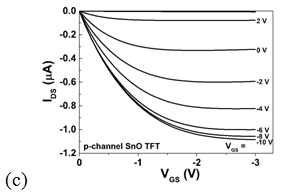
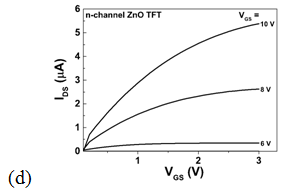
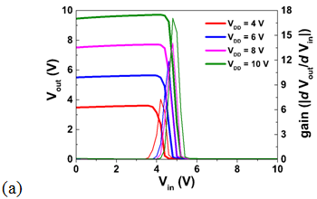
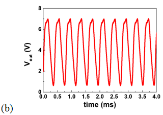
Complementary thin-film transistor (TFT) circuitry consisting of inverters is the building block for realizing integrated logic circuits on large-area and/or flexible substrates. Although numerous oxide-TFT circuits have been reported previously, most of them were based on n-channel MOSFET (NMOS) technology, implying that the development of p-channel oxide-TFTs with sufficient satisfactory performance via a low-temperature process is crucial. In this study, we report, for the first time, fully oxide-TFT-based complementary metal-oxide-semiconductor (CMOS) ring oscillators by using large–area-compatible sputtering processes. The p-channel tin monoxide (SnO) and n-channel zinc oxide (ZnO) TFTs used in the CMOS inverter have inverted-staggered bottom-gate structures. The SnO TFT exhibits a threshold voltage (Vth) of 3.5 V, field-effect mobility of 0.33 cm2/V-s, sub-threshold swing (S.S.) of 2.5 V/decade, and on/off current ratio of ~103. The corresponding values for the ZnO TFT are 6.22 V, 3.5 cm2/V-s, 350 mV/decade, and >106. The achieved voltage gain of the CMOS inverters is ~17 at a supplied voltage (VDD) of 10 V when the geometric aspect ratio is 5. An oscillation frequency of 2 kHz is obtained from a five-stage oxide-based CMOS voltage control oscillator at VDD of 14 V. The result shows the feasibility of realizing fully oxide-TFT-based CMOS circuits.
|
|
 |
|
Fig. 2 (a) The static voltage transfer characteristics and voltage gain curves at different supply voltages (VDD) of the complementary oxide-TFT inverter with a geometric aspect ratio, (W/L)p/(W/L)n, of 5. (b) Output waveform of a five-stage ring oscillator based on complementary oxide-TFT inverters at VDD = 14 V. |
Development of numerical modeling program for organic/inorganic hybrid solar cells by including tail/Interfacial states models
Professor Yuh-Renn Wu
Graduate Institute of Photonics and
Optoelectronics, National Taiwan
University
A simulation software is developed for modeling the organic/inorganic hybrid solar cells. Firstly, the optical field in the solar cell device is calculated by using the two-dimensional finite-difference time-domain (2D-FDTD) method. By solving the Poisson’s and drift-diffusion equation which utilizes the finite element method (FEM), the electrical properties of the device can be obtained. A Gaussian distribution function of tail states is addressed to simulate the carrier transportation in the organic material. These tail states located around the lowest unoccupied molecular orbital (LUMO) and the highest occupied molecular orbital (HOMO) of the organic material provides a path way for carriers to hop in and transport through the organic material. In this research, a poly(3,4-ethylenedioxythiophene):poly(4-styrenesulfonate) (PEDOT:PSS)/silicon nanowire (SiNW) hybrid solar cell is set up as the simulation model. The validity of the software is verified by comparing the simulated J-V curve with experimental J-V curves. The electrical and optical properties are analyzed for further optimization.
|
|
|
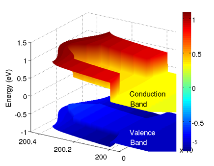
Fig. 1. The simulated band diagrams of the PEDOT:PSS/SiNW hybrid solar cells. |
|
|
|
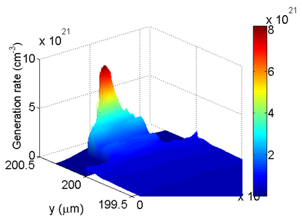
Fig. 2. The generation rate of the PEDOT:PSS/SiNW hybrid solar cells calculated by 2D-FDTD. |
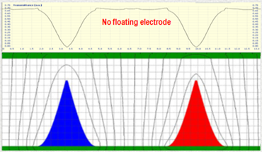
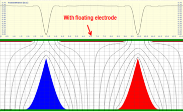
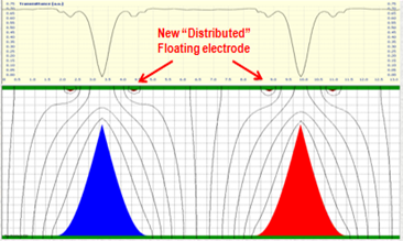
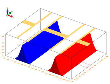
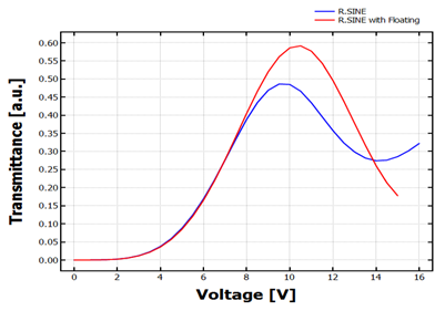
Polymer-Stabilized Blue-Phase Liquid Crystal Display Using Distributed Floating electrode
Professor Wing-Kit Choi
Graduate Institute of Photonics and
Optoelectronics, National Taiwan
University
We have recently proposed a new electrode design for a Polymer Stabilized Blue Phase Liquid Crystal (PS-BPLC) display based on floating electrode [1]. We name it “distributed floating electrode design”. In this new design, we can use less area of floating electrode while still achieving the similar increase of the overall light transmission as in the previously proposed structure [2]. Our new design may have the potential to help reduce the image sticking problem that may be caused by the use of floating electrode and also further improve the light efficiency due to the use of less ITO area. Due to its attractive features such as i) fast response time, ii) no need of alignment layers and iii) wide viewing angle property, PS-BPLC has been proposed and actively researched as the next generation display technology in recent years.
Reference: [1] Y.C. Chang, S.H. Wei, C.L. Chang and W.K. Choi, “Polymer-Stabilized Blue-Phase Liquid Crystal Display Using Distributed Floating electrode”, Society for Information Display (SID), 2016, [2] Y. Liu, Y. Li, D. Lai, J.W. Shiu and S.T. Wu, “High Transmittance Blue-phase LCD with a Floating Electrode” Society for Information Display (SID), 2013
1.1 μm InAs/GaAs quantum-dot light-emitting transistors grown by molecular beam epitaxy
Professor Chao-Hsin Wu
Graduate Institute of Photonics and
Optoelectronics, National Taiwan University
We report the enhanced radiative recombination output from an AlGaAs/GaAs heterojunction bipolar transistor with InAs quantum dots embedded in the base region to form a quantum-dot light-emitting transistor (QDLET) grown by molecular beam epitaxy
systems. For the device with a 100×100 μm2
emitter area, we demonstrate the dual output
characteristics with an electrical output and an
optical output when the device is operating in
the common-emitter configuration. The
quantum-dot light-emitting transistor exhibits a
base recombination radiation in the
near-infrared spectral range with a dominant
peak at
λ
of 1100 nm. This work has been published in
Optics Letters, Vol. 40, No. 16, pp. 3747,
(2015).
|
|
|
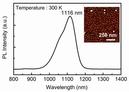
Fig. 1. The atomic force microscopic image (inset) and photoluminescence (PL) spectrum of the InAs/GaAs QDLET at 300 K with 4 mW/cm2 excitation power. The PL peak at 1116 nm indicates the transitions of carriers on predominant InAs QDs. |
|
|
 |
|
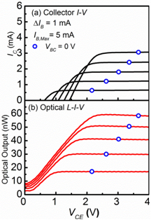
Fig. 2. (a) Electrical I-V and (b) optical L-I-V of the InAs/GaAs QDLET with a 100×100 μm2 emitter area. The blue circles indicate the VBC = 0 V points. |
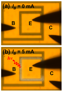
Fig. 3. (a) Top view layout of the InAs/GaAs QDLET and (b) CCD image of the infrared light emission when transistor operates in the common-emitter configuration (IB = 5 mA, VCE = 4 V). |
|
|
|
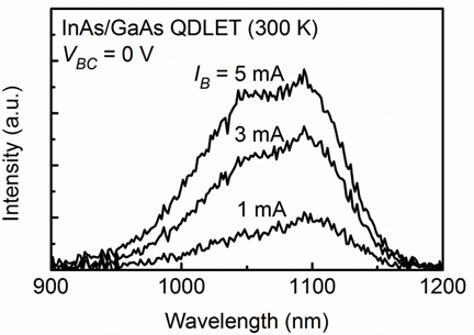
Fig. 4. Electroluminescence spectrum of the InAs/GaAs QDLET at different base currents. The wavelength peaks are at 1100 nm corresponding to the radiative recombination contributed from the InAs QDs. |
Dual-functional Memory and Threshold Resistive Switching Based on the Push-Pull Mechanism of Oxygen Ions
Professor Si-Chen Lee’s laboratory
Graduate Institute of Photonics and
Optoelectronics, National Taiwan
University
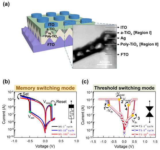
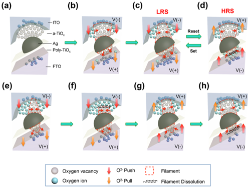
The resistive random access memory (RRAM) becomes more and more important as the candidate to overcome the technological limitations for next-generation non-volatile memory. We have developed a special device structure (a-TiOx)/(Ag NPs)/(poly-TiOx) sandwiched between indium tin oxide (ITO) and fluorine-doped tin oxide (FTO) electrode as shown in Fig. 1 (a) which performs dual functions, i.e., memory switching (RRAM device) and threshold switching (Selector device). When used for memory switching, the device is forming-free with low operation voltage (< ±1 V) and self-compliance to current up to 50 μA as shown in Fig. 1(b). This reduced the damage of forming process on the device endurance. When the device is used for threshold switching as shown in Fig 1(c), the reduction of the threshold currents to -2 μA and 0.1 μA in negative and positive voltage regions, respectively, is beneficial for improving the device selectivity to solve the sneak current problem in the crossbar memory arrays. It is found that the push and pull actions of the oxygen ions in the top amorphous and bottom polycrystalline TiOx films due to voltage sweeps can account for the dual-functional properties in a single device structure, as illustrated in Fig. 2.
|
|
|
Fig. 1. Device structure and electrical properties of the dual functional switching device. |
|
 |
|
Fig. 2. Push-pull mechanism of oxygen ions migration in the memory switching and threshold switching modes. |
Y. J. Huang, S. C. Chao, D. H. Lien,
C. Y. Wen, J. H. He and S. C. Lee,
“Dual-functional Memory and
Threshold Resistive Switching Based
on the Push-Pull Mechanism of Oxygen
Ions”,
Nature Sci. Rep.
6, 23945, 2016.
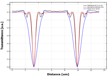
Multi-Bent-Section Nano-Antennas
Professor Hung-chun Chang
Graduate Institute of Photonics and
Optoelectronics, National Taiwan
University
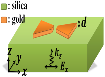
Nano-antennas are a class of nano-structures that can produce “hot spots” in a subwavelength gap of the structure due to plasmonic effects under incident electromagnetic fields and have been extensively investigated in the visible and infrared wavelength range both theoretically and experimentally. Bowtie nano-antennas or bowtie antennas (BAs), as depicted in Fig. 1, have been a popular structure. The resonant wavelength
λres
of the BA is proportional to the antenna length. For a given footprint size, achieving longer
λres is useful in applications within the near- or mid-infrared range. We have recently proposed multi-bent-section nano-antennas (MBSNAs) which are dipole nano-antennas with multi-bent-sections and demonstrate that such simple structures can achieve long
λres’s with high gap fields. The study was based on our in-house developed 3D finite-difference time-domain (FDTD) method [IEEE Photon. J.
7, 4501108 (2015)]. Referring to the BA of Fig. 1 as the basic structure, the bowtie-shaped gold film with thickness
d is supported by a silica substrate with relative permittivity of 2.25, and it is air above the structure. The function of the gold is described by the Drude model [Phys. Rev. B.
71, 085416 (2005)]. The antenna footprint area is kept the same to be 450 nm × 450 nm, with the thickness
d
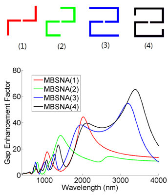
fixed to be 36 nm and the antenna gap area fixed to be 30 nm × 30 nm. Four MBSNAs with different shapes of the gold region as shown in the top of Fig. 2, each with the same
d
and the gap area as aforementioned, have been simulated. Every section of each antenna is with the same width of 30 nm. It can be seen the antenna structure is very simple even for the fourth one. The results of Fig. 2 is to be compared with the reference BA for which the resonance occurs at
l
= 1260 nm and the corresponding gap-field enhancement is 31. The proposed structures are also with wide bandwidth in the enhancement spectrum. By numerically solving the modal effective indices of the plasmonic waveguide having its cross-section as that of the gold line with the substrate of the MBSNA, the
λres’s for the bent gold-line waveguide length were determined and found to be in good correlation with those of the peaks in Fig. 2. (Yu-Tsung Chen and Hung-chun
Chang, in Proc. OPTIC 2015 .)
|
|
|
Figure 1. Schematic of the 3-D representation for a bowtie nano-antenna. |
|
 |
|
Figure 2. Upper part: four different shapes of the gold region of the MBSNAs. Lower part: Gap enhancement factor versus the wavelength for the four MBSNAs. Each MBSNA has the same footprint size of 450 nm × 450 nm. |
|
|
|
|
|
|
|
| |
|
|
 |
|
 |
|
|
|