Latest News Special Report Research Result Column Laboratory Descriptions
![]() Beginning August 1st, 2007, GIPO professor Gong-Ru
Lin as GIPO Vice Chairman to assist in GIPO affairs
Beginning August 1st, 2007, GIPO professor Gong-Ru
Lin as GIPO Vice Chairman to assist in GIPO affairs
|
With 34 professors and 350 graduate students, GIPO is a busy and dynamic institute that needs a vice chairman to assist in managing its affairs. Aside from being a GIPO professor, Professor Gong-Ru Lin is also an active member of the academic society of photonics. He is currently the vice president of IEEE/LEOS Taipei Chapter and SPIE Taiwan Chapter. Professor Gong-Ru Lin has made great achievements in the area of research; he received the Third Best Scientific and Technical Paper Award (with co-authors) from the Far Eastern Y. Z. Hsu Science |
 |
|
& Technology Memorial Foundation of R. O. C. in 2004, the Young Scholar Research Award from NCTU in 2005, and the Award of Outstanding Youth Electrical Engineer from SIEE in 2005. Prof. Lin has published over 200 research papers in international journals and conferences. GIPO’s Vice Chairman will act as head of the Institute when the chairman is out of the country or unable to perform the duties. |
|
![]() GIPO
Academic
Visiting
Highlights
GIPO
Academic
Visiting
Highlights
|
June “Photonics Forum” Lecture Highlights |
|||
|
Time: June 15th, 2007, 4:30 pm Speaker: Dr. Gerd Keiser (University of Wisconsin-Milwaukee) Topic: An Overview of Biophotonics Dr. Gerd Keiser visited GIPO on June 15th, 2007 (Friday), and lectured in the auditorium 101 in Barry Lam Hall. The lecture “An Overview of Biophotonics” was attended with enthusiasm by GIPO professors and students. |
|
||
|
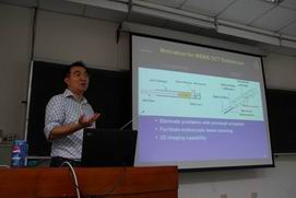
July GIPO Lecture Highlights Time: July 27th, 2007, 4:30 pm Speaker: Professor Chinlon Lin (Professor of Photonics and Director, Center for Advanced Research in Photonics, Depts. of Electronic Engineering and Information Engineering, Chinese University of Hong Kong ) Topic: Photonics for Optical Networks and Fiber-to-the-Home—The Broadband Transformation |
|||
|
|||
|
August GIPO Lecture Highlights |
|||
|
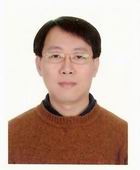
Time: August 17th, 2007, 10:00 am Speaker: Dr. Wibool Piyawattanametha (Physical Science Research Associate, Stanford University) Topic: Advanced Endoscopy/Microscopy Dr. Wibool Piyawattanametha visited GIPO on August 17th, 2007 (Friday) and gave a lecture in room 145, the EE Building II on the topic of “Advanced Endoscopy/Microscopy”. GIPO professors and students learned much from the lecture. |
 |
||
![]() Program for
Graduate Student Exchange
Program for
Graduate Student Exchange
between National Taiwan University and National University of Singapore
![]()
【Optoelectronics Student Exchange Workshop】
June 26th to July 1st, 2007
National University of Singapore
Highlight Compilation: GIPO Ph.D. candidate Sen-Ming Hsu
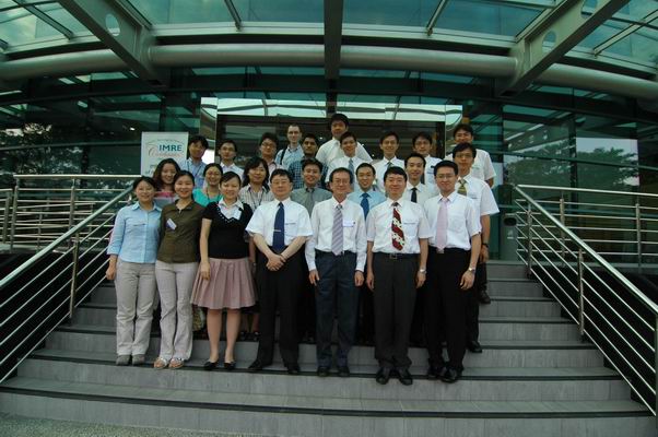
On January 26th, GIPO announced the list of the eight Ph.D. candidates chosen as part of the representative group that would include Chairman C. C. Yang, Vice Chairman Sheng-Lung Huang to attend the Graduate Student Exchange with the National University of Singapore taking place in the latter half of June. Since that day, the chosen Ph.D. candidates all felt honored at such an opportunity to represent GIPO in the exchange with the National University of Singapore. The representative group held its first pre-trip meeting on April 27th, and elected student group leader Chi-Feng Huang, and associate group leader Tien-Lung Chiu, who would be responsible for making necessary arrangements with the National University of Singapore student representatives. After four pre-trip meetings, the representative group left Taiwan on June 26th for Singapore to participate in the exchange, lasting six days and five nights.
The Optoelectronics Student Exchange Workshop, which took place on June 27th, marked the beginning of the exchange between the participating parties. GIPO Chairman C. C. Yang made opening remarks, followed by the presentations given by Prof. S. J. Chua of NUS and Prof. S. L. Huang of NTU, each of whom introduced the related research institutes within his own university. Next, student representatives from both parties reported on their personal research accomplishments and those of their laboratories. Topics reported included crystal growth, processing, characterization, and model design, etc. Participants and speakers from both groups entered discussions with enthusiasm, indicating that both parties thought highly of this conference.
During the two days following the successful conclusion of the conference, the Singapore party thoughtfully arranged visits to the photonics laboratories at National University of Singapore and other important organizations and laboratories involved in photonics related research, including Institute of Material Research and Engineering, Silicon Nano Device Lab, Center for Optoelectronics, Data Storage Institute, Laser Micro Processing Lab, Singapore Institute of Manufacturing Technology, and Institute of Microelectronics. During the visits, members of the NTU representative party were left with deep impressions of Singapore’s research environment, instruments and facilities. The members also learned much about the management and development of laboratories and gained much knowledge from this trip.
Firstly, great thanks to Chairman C. C. Yang and Vice Chairman Sheng-Lung Huang for the successful completion of this trip. During every pre-trip meeting discussion, and every exchange activity, both professors worked hard to guide and assist the students of the representative group. Also, thanks to student representatives of both parties for organizing the event, and to Ms. Hsiao-Wen Lin, who aided in communicating and arranging related affairs. Finally, special thanks to NTU for providing the representative party with the financial support for this exchange event and for helping us bring it to the successful conclusion.
 |
|
The professors and students of both participating parties |
![]() Research Result Column for the Program of
“Aiming for Top University”
Research Result Column for the Program of
“Aiming for Top University”
Research of Organic Light Emitting Materials
Professor Chih-I Wu
Graduate Institute of Photonics and Optoelectronics, National Taiwan University
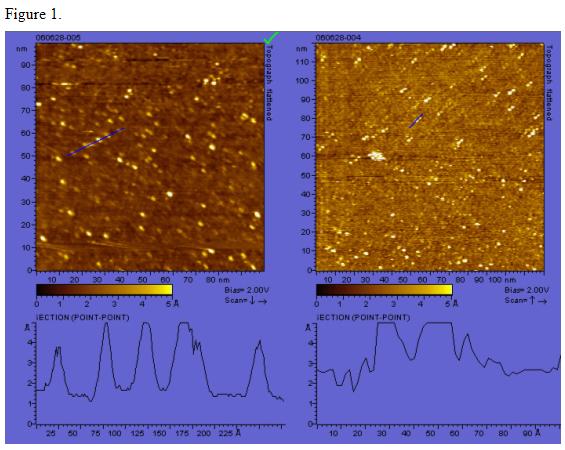
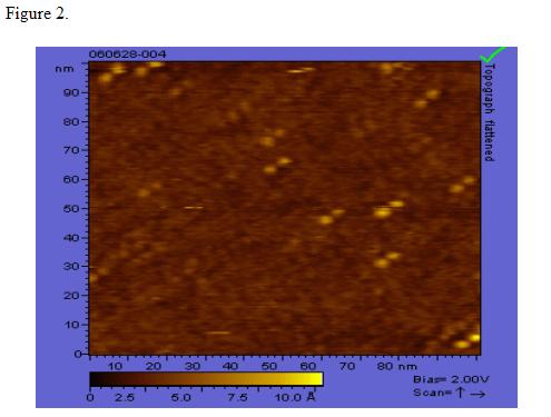
In the previous year, we have been working on the investigation of the arrangement and orientation of the organic thin films deposited on various surfaces. We have probed the organic molecular arrangement at the substrate in nano-scale with scanning tunneling microscope (STM). We deposited less than 0.1 mono-layer of NPB on silicon surface and investigate with STM. As shown in Figure 1, the NPB molecules can be seen clearly as the bright spots on the surface. The NPB molecules are evenly spread on the surface of the substrate. More amazingly, some of the molecules are form as dimers as shown in the Figure 2. The underlying interaction and physics of the formation of the dimers will be investigated this year.
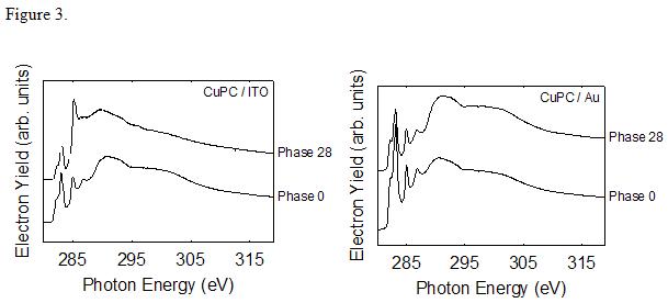
We also perform the photoelectron emission microscopy (PEEM) at National Synchrotron Radiation Research Center (NSRRC) to investigate the orientation of the organic electronic films on different substrates. Figure 3 shows the PEEM spectra of CuPc on ITO and Au surfaces. Form the spectra we can determine that CuPc molecules lie flatly on the Au surfaces, whereas the same molecules arrange perpendicular to the ITO surface with the same deposition condition. The result demonstrate that we can use PEEM to determine the stacking arrangement of the organic molecules at the surfaces with PEEM, which can be a good complement technology to STM and very useful to this nanotechnology projects.
 |
 |
 |
![]()
![]()
Pseudopsectral Time-domain Simulation—
A Virtual Optical Experiment for Tissue Optics
Professor Snow H. Tseng
Graduate Institute of Photonics and Optoelectronics, National Taiwan University
Optical diagnostic techniques are developed based upon an understanding of the propagation of light through tissue structures. However, to date, most optical models are based upon heuristic approximations. We propose a virtual optical experiment by implementing the pseudospectral time-domain (PSTD) algorithm on parallel computers. By means of the proposed virtual optical experiment, we investigate the phenomenon of light scattering by a macroscopic cluster of randomly-positioned dielectric spheres. The transition of the optical properties from sparse scatterers to closely packed scatterers has been investigated. Research findings suggest that light scattering by a closely packed random medium should be treated as a whole, rather than a sum of consecutive series of independent scattering events. More importantly, the proposed virtual optical experiment is applicable to macroscopic, arbitrary geometry, providing a robust research tool for tissue optics.
|
|
|
Fig. 1. PSTD-computed total scattering cross-section (TSCS) spectra of a cluster with an overall diameter D = 50 mm, consisting of N randomly positioned, non-contacting, n = 1.2 dielectric spheres of individual diameter d = 10 mm. Five cases are shown (bottom to top): N = 5, 15, 30, 50, and 56. As more and more spheres are packed together, the optical characteristics due to the overall geometry becomes more pronounced and gradually dominate the characteristics of individual spheres. |

![]()
![]()
Organic Deformable Mirror
Professor Guo-Dung Su
Graduate Institute of Photonics and Optoelectronics, National Taiwan University
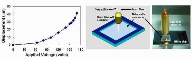
Erbium-doped fiber amplifiers have made long-haul WDM transmission practical. Fiber amplifiers do permit multi-channel transmission, but it is critical to maintain signal integrity for all channels after cascading a number of fiber amplifiers. Variable optic attenuator (VOA) is the device that manages signal power in fiber optic links by inducing variable loss. It is used to control the power level of optical signals between outputs of light sources and electrical-to-optical (E/O) converters. It can also be applied to test the linearity and dynamic range of photo sensors and photo detectors. Fiber variable optical attenuator (VOA) has been previously realized by means of liquid crystal, acousto-optic, and MEMS (Micro-Electro-Mechanical Systems) devices. Due to recent fast progress in micromachining fabrication, VOA made by MEMS technology shows high reliability and compact size, which make MEMS VOA promising for telecommunication applications. It was proposed to implement VOA by the optical beam spoiling method and 3-D beam spoiling was realized via a simple micro-machined deformable mirror device that changes the focal length of a membrane. The previous membrane approach, however, was made by brittle semiconductor materials. The stroke was generally limited to less than 10 μm, and the highest attenuation was restricted to less than 5dB.
In our lab, we have fabricated a novel MEMS VOA consisting of a deformable polyimide thin film aligned with a fiber collimator in a free-space configuration. Due to the compliant structure of an organic thin film, the deformation of an organic thin film can attenuate the light intensity > 15-dB with 0.01-dB resolution at the wavelength of 1550 nm. Its surface roughness was measured about 20 nm and the insertion loss caused by the membrane is 0.46 dB. The load-deflection experiment result shows significantly low residual stress of 3.2 MPa and Young’s modulus of 15 GPa The deformation of the membrane is up to 41 μm without permanent warps, and the membrane size is 6mmX6mm separated from a bottom electrode by 70 μm. It can be potentially applied to many other optical applications.
 |
![]()
![]()
Carrier Transport and Recombination in Mixed-host Organic Light-emitting Device
Professor Jiun-Haw Lee
Graduate Institute of Photonics and Optoelectronics, National Taiwan University
Carrier transport and recombination in a mixed-host organic light-emitting device (OLED) can be determined by fitting the current-voltage characteristics and inserting a thin probe at different positions of the device. Furthermore, the latter approach increases the recombination current and improves the power efficiency.
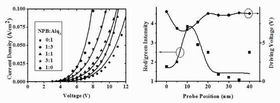
We used N,N’-diphenyl-N,N’-bis(1-napthyl)-1,1’-biphenyl-4,4’-diamine (NPB) as the hole transport layer (HTL) material and tris-(8-hydroxyquinoline) aluminum (Alq3) as the electron transport layer (ETL) material. The bipolar emitting layer (EML) was a mixture of NPB and Alq3 with different mixed-ratios. Fig. 1 shows the experimental and simulated J-V characteristics. The driving voltage increased and then decreased with increasing the NPB concentration. Raising NPB concentration leaded to the enhanced hole-current and reduced electron-current. The hole-current enhancement did not compensate the electron-current decline when the HTL ratio increased from 0 to 25%. The sequential increase of HTL material concentration from 25 to 100% resulted in the voltage reduction on account of rapidly boost of hole-current.
Besides, we inserted a very thin 4-(dicyanomethylene)-2-tert-butyl-6-1,1,7,7- tetramethyljulolidyl-9-enyl)-4H-pyran (DCJTB) layer (1.2 nm) with 2 vol. % in different positions of the EML layer (NPB:Alq3=1:1) to detect the distribution of the recombination-rate. In Fig. 2, we show that the relative intensity of probe/matrix at 2.5 mA/cm2 and the driving voltage at 100 mA/cm2 as a function of the probe positions. The curve of driving voltage versus probe position is almost the inverse of that of intensity ratio. The position of the maximum red/green ratio and the minimum driving voltage are 10 nm from the HTL/EML interface. This phenomenon is attributed to the higher recombination rate of the high-quantum-yield red dopant than that of the matrix, and thus driving voltage decreases due to the increase of the recombination current.
 |
|
|
Figure 1 Experimental (dots) and stimulated (solid lines) J-V characteristics of different mixing ratios. |
Figure 2 (Squares) Intensity of red/green ratio versus probe position at 2.5 mA/cm2. (Circles), and driving voltage at 100mA/cm2 versus probe position. |
![]()
![]()
Flexible Thin Film Transistors
Professor I-Chun Cheng
Graduate Institute of Photonics and Optoelectronics, National Taiwan University
Flexible electronics are under intense research today because they possess desirable features of lightweight, ruggedness, and flexibility. To realize these flexible electronics, a flexible transistor backplane is the basic requisition. We have been working on amorphous silicon thin film transistors (TFTs) made on glass and flexible organic polymer foil substrates. The TFTs have staggered, bottom-gate geometry with back-channel cut. Both as-fabricated TFT performances and bias-stress stabilities are investigated. It has been found that the TFT performances as well as stabilities are primarily dependent on the processing temperatures, not a function of substrate types.
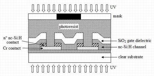
We also explore the nanocrystalline silicon (nc-Si:H) thin film transistor, which is a potential candidate for high performance flexible electronics. This is particular interesting because it can be made in a way which is fully compatible with present a-Si:H technology. The TFTs are fabricated in a staggered top-gate, bottom-source/drain geometry on top of a nc-Si:H seed layer. The top-gate geometry is adopted to take advantage of the high carrier mobilities available at the top of nc-Si:H films, and the seed layer is used to promote rapid nucleation of the channel layer. Self-alignment process is also applied to the nc-Si:H TFTs by combining back-side photolithography with lift-off patterning of the top-metal contacts. The self-aligned nc-Si:H TFTs have similar characteristics to that of their non-self-aligned counterpart, which indicates that the UV exposure through the nc-Si:H channel does not cause significant degradation.
 |
|
Figure 1. Self-aligned photolithography process for nc-Si:H TFTs with staggered top-gate, bottom-source/drain geometry. |
![]()
![]()
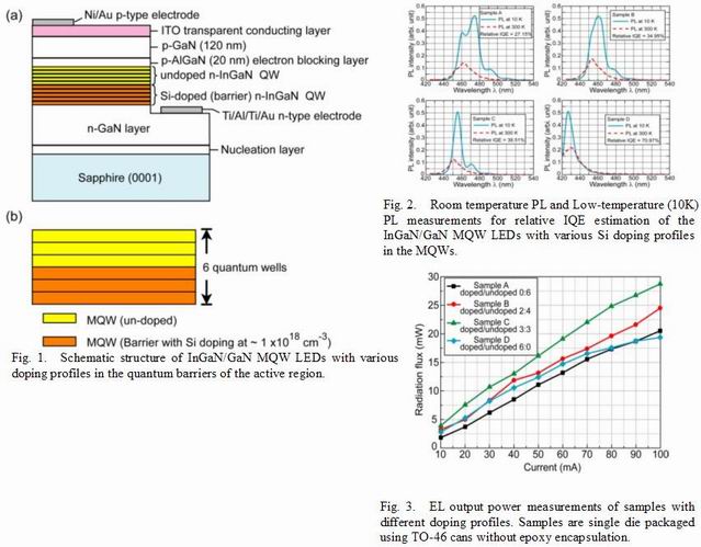
Performance of InGaN/GaN multiple-quantum-well light-emitting diodes with different Si doping profiles
Professor Yun-Li Li
Graduate Institute of Photonics and Optoelectronics, National Taiwan University
III-nitride based high-brightness light-emitting diodes (LEDs) have attracted a lot of attention due to their various applications on signage, back-lighting and illumination applications. Many efforts have been made to improve material quality, light extraction efficiency, and metal-semiconductor ohmic contacts so that emission efficiencies of LEDs based on this material system have improved drastically.
In this study, different Si-doping profiles for the barriers of InGaN/GaN MQW LEDs are investigated and the measurements of the electrical and optical performance of these LEDs are discussed. Investigation of IQE results indicates that with an increasing number of doped barriers, the internal quantum efficiencies increase owing to the compensation of QCSE and higher carrier densities. However, after LED chip fabrication and single die packaging without epoxy encapsulation, the EL radiation flux measurements show that when the number of doped-barriers increases, early radiation flux saturation and low external quantum efficiencies are found under high current injection.
 |
|
Flexible Optoelectronics Laboratory Research Fields: 1. Nanocrystalline silicon thin film technology 2. Display technology: Flexible thin film transistor backplane technology 3. Stability study of flexible thin film devices |
|
1. Introduction
The major research fields in our lab are nanocrystalline silicon thin film technologies and flexible electronics and optoelectronics, including design, fabrication and stability study of these devices. These flexible devices possess desirable features, such as light weight, ruggedness, flexibility and even deformability. Examples of their applications include solar cell, flexible displays, display wallpaper, rugged X-ray sensor arrays, smart textile, and etc. The basic idea of this technology is combining existing electronic and optoelectronic devices with flexible substrates. This field has open boundaries that move with its development and application and been gradually integrated into the design of next generation large area electronic products.
2. Current research subjects
(1) Nanocrystalline silicon thin film technology
Hydrogenated nanocrystalline silicon has been considered as a potential material in large area electronic and optoelectronic applications. Examples include thin film solar cell, thin film transistors, and etc. We have been exploring hydrogenated nanocrystalline silicon (nc-Si:H) based on its (i) high electron field effect mobilities compared to a-Si:H, (ii) capability of p-channel operation, (iii) low process temperature, and (iv) compatibility plastic substrates, and (v) compatibility with current hydrogenated amorphous silicon technology. The film can be obtained by plasma enhanced chemical vapor deposition. The film crystallinity and grain sizes, usually ranges from couple nanometers to tenth of nanometers, are strongly dependent on the deposition conditions, such as gas composition. The influence of nc-Si:H crystallinity on its optical and electrical properties is one of the important subject we are working on now.
(2) Flexible thin film transistor backplane technology
Transistor backplane is one of the major components in flat panel display. It has the function of switching and/or driving the front panel materials. The active material in the flexible thin film transistor backplane can be divided into two groups: organic and inorganic materials. Our research has focused on combining silicon-based inorganic materials with flexible substrates. Silicon-based inorganic thin film has the advantages of high compatibility with well-established silicon technology and good chemical and electrical stabilities. However, due to the mismatch of the mechanical properties between the inorganic thin films and the organic polymer substrates (plastics), thin film fracture and stress induced problems are often encountered during device fabrication and operation. To overcome these challenges is another important task in our lab.
(3) Stability study of flexible thin film devices
Plastic substrates demand ultralow process temperature. However, depositing silicon-based materials at temperatures of 200°C or below often brings up degradation of film qualities, such as increase of sub-bandgap defects. The change of sub-bandgap defect density can further influence the stability of devices. The goal of our research is to have a fundamental understanding of these silicon-based materials by systematic study of the correlation among thin film structure/phase, subbandgap defect density distribution, and stability behavior of the corresponding devices.
|
Liquid Crystal Display Technology Laboratory Current & Prospective Research Areas: 1. Transflective TFT-LCDs 2. Fast Response Time technologies 3. Wide Viewing Angle technologies 4. Novel Liquid Crystal electro-optic effects |
|
I. Background
The current research activities of this laboratory focus on the development of Transflective TFT-LCDs (TR-LCDs) which have, in recent years, become a very important display mode for small to medium sized portable electronic devices such as cellular phones, PDA, MP3, digital cameras etc.. The main advantage of TR-LCDs over the conventional transmissive-type TFT-LCDs is that the former is capable of displaying legible images under any illumination conditions, i.e. suitable for both indoor and outdoor usages.
II. Research Objective
Due to the optical-path difference between the transmitted and reflected lights, majority of TR-LCDs at present are based on the rather complicated “double-cell-gap” structure, which requires a more demanding fabrication process control and hence often leads to lower production yields and higher manufacturing cost. Moreover, this structure also exhibits other undesirable features such as unequal response time between transmitted and reflected images, reduced aperture and very often limited viewing-angle characteristics. The main objective of our research is thus to develop new or novel designs of TR-LCD which can allow a simpler structure, more cost-effective fabrication process and improved optical properties. The design and optimization process of these new displays are being developed through the use of professional Liquid Crystal Display Modeling software Dimos and 2DimMos that we purchased from autronic-Melchers, Germany. Advanced wide-viewing-angle and fast-response-time LCD technologies such as IPS, PVA & OCB are also being investigated and developed for application in these new TR-LCDs and other future-generation TFT-LCDs.
|
Biophotonics and MEMS Design Laboratory |
|
|
|
Front row, right: Prof. Jui-che (Ted) Tsai;Front row, left: Dr. Chia-Wei Sun, ITRI |
The researches in our group include optical MEMS and biophotonics. Below are a few selected topics.
Linearization of a MEMS scanner
A differential-voltage driving scheme is developed to linearize the dc characteristic (angle vs. voltage) of a MEMS scanner. The two polarities of the differential voltage VDifferential are superimposed on a dc bias voltage VDC, respectively. The resulting sum voltages, (VDC+VDifferential) and (VDC-VDifferential), are applied on opposite electrodes. The bias voltage is scanned so that the optimal operation point can then be determined. The control voltage, VDifferential, is tuned within the range of ±10V, eliminating the use of power amplifiers.
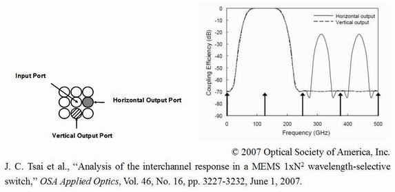
Analysis of the interchannel response in a MEMS 1xN2 wavelength-selective switch
A theoretical model based on Fourier optics and the power-coupling overlap integral is built to investigate the inter-channel response in a MEMS 1xN2 wavelength-selective switch (WSS). The inter-channel response is undesirable in WDM systems. Simulation results demonstrate that it depends significantly on the output port location and the radius of curvature of the micromirrors. Therefore, the inter-channel response can be suppressed by adjusting the output port locations.
 |
Diffuse Optical Tomography
Recently, diffuse optical tomography (DOT) has been demonstrated as an effective tool for image construction of brains, breasts, and joints, etc. Near-infrared lights penetrate several centimeters into the tissue to measure the spatial distribution of absorbance. Since oxy-hemoglobin (HbO2) and deoxy-hemoglobin (Hb) exhibit different absorption spectrum, the spatial distributions of HbO2 and Hb can be derived from the measured absorbance distributions for two or more various optical wavelengths. Observations of the HbO2 and Hb distributions help to diagnose many early-stage diseases.
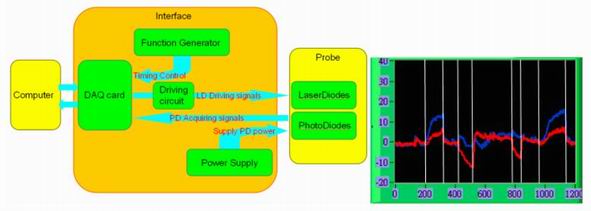
For the DOT research, we collaborate with Dr. Chia-Wei Sun of Medical Electronics and Device Technology Center, Industrial Technology Research Institute (ITRI). Conventionally, DOT systems are implemented with fiber optics and are usually bulky. Moreover, the coupling of light from tissue into fibers results in optical loss and therefore degrades the signal-to-noise ratio (SNR). We, on the other hand, attach 6 pairs of laser diodes and 12 photo detectors directly on an 8.5cm x 8.6cm flexible printed circuit board. Each pair of laser diodes consists of a 780 nm and an 850 nm light source. During measurement, the printed circuit board is adhered directly to the tissue surface. This approach eliminates the use of optical fibers, reduces the cost, increases the system compactness and portability, and improves the SNR and image quality. The system block diagram and the measured clinical signals are shown below.
 |
We have successfully obtained preliminary clinical results. In the future, we expect to employ DOT in brain function characterization and diagnosis of cardiovascular diseases.
Please send any comment to GIPO_5@cc.ee.ntu.edu.tw
Copyright
Graduate Institute of Photonics and Optoelectronics, National Taiwan University