Latest News Special Report Research Result Column Profiles Laboratory Descriptions
![]() Congratulations! GIPO Distinguished Research Fellow Chen-Shui
Tsai was awarded 2007 NTU’s Outstanding Alumnus in the Academic Category.
Congratulations! GIPO Distinguished Research Fellow Chen-Shui
Tsai was awarded 2007 NTU’s Outstanding Alumnus in the Academic Category.
|
The recipients of 2007 NTU’s Outstanding Alumnus has been announced. This year’s award categories are Arts and Literature, Academics, Business, and Social Service. Nine alumni have been awarded. GIPO Distinguished Research Fellow Chen-Shui Tsai was awarded the Outstanding Alumnus in the Academic Category. Congratulations! This year’s Outstanding Alumnus recipients were commended during NTU’s anniversary celebration on November 15th. For details, please visit http://homepage.ntu.edu.tw/~ntualumni/board/96.10.25new.html. |
 |
![]() Congratulations! Professor Chung-Chih Wu’s National Science
Council (NSC) research project has achieved outstanding results.
Congratulations! Professor Chung-Chih Wu’s National Science
Council (NSC) research project has achieved outstanding results.
|
Professor Chung-Chih Wu executed the National Science Council (NSC) research project “Photonic Devices and Photonic Characteristics Simulation Design Technology”, and received a royalty of one million NTD. Congratulations on achieving such outstanding research results! |
 |
![]() GIPO, National Taiwan University and Faculty of Physics, M.V.
Lomonosov Moscow State University signed an agreement for scientific and
educational cooperation.
GIPO, National Taiwan University and Faculty of Physics, M.V.
Lomonosov Moscow State University signed an agreement for scientific and
educational cooperation.
|
Through Professor Lung-Han Peng’s arrangement and coordination, an agreement for scientific and educational cooperation was signed by GIPO, National Taiwan University and Faculty of Physics, M.V. Lomonosov Moscow State University on November 23rd, in the 7F conference room of Barry Lam Hall. The agreement outlines the reciprocal exchange program of cooperation in academic teaching and research. |
![]() GIPO
Academic
Visiting
Highlights
GIPO
Academic
Visiting
Highlights
|
September GIPO Lecture Highlights |
|
|
Time: 4:00 pm, September 26th, 2007 Speaker: Dr. Lars Zimmermann (Technical University of Berlin) Topic: Silicon-on-Insulator Rib-Waveguide Technology Dr. Lars Zimmerman visited GIPO on September 26th, 2007 (Wednesday) and gave a lecture in room 142, the EE Building II on the topic of “Silicon-on-Insulator Rib-Waveguide Technology”. GIPO professors and students attended with enthusiasm and learned much from the lecture. |
|
|
November “Photonics Forum” Lecture Highlights |
|
|
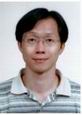
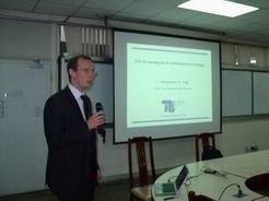
Time: 4:00-6:00 pm, November 16th, 2007 Speaker: Dr. Chen-Shui Tsai (Academician of Academia Sinica) Topic: A Progress Report on Silicon-Based Ultrasonics and Photonics Research Dr. Chen-Shui Tsai, Academician of Academia Sinica, visited GIPO on November 16th, 2007 (Friday) and gave a lecture in the Auditorium 101 in Barry Lam Hall. His lecture, “A Progress Report on Silicon-Based Ultrasonics and Photonics Research”, was attended by GIPO professors and students with enthusiasm. |
 |
| Right: Prof. Tsai; Left: Prof. Tsai's wife, Prof. Shirley Tsai. | |
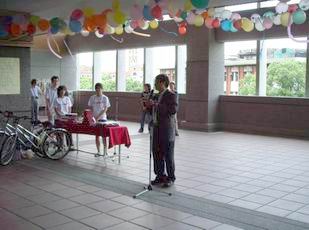
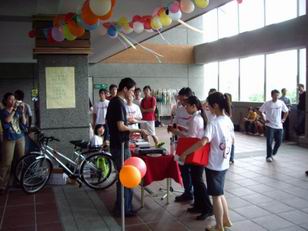
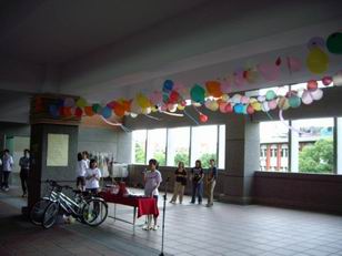
![]() GIPO Student Association’s
GIPO Student Association’s
2007 Welcome Party and Mid-Autumn Festival Lunch Party
![]()
September 21st, 2007
3F, Central Plaza, Ming-Da Hall, NTU
Jun-Xiang Yan, President of GIPO Student Assocation
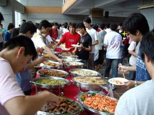
This year’s annual Mid-Autumn Festival lunch party was the first major GIPO student event of the academic year.
 |
 |
|
Distinguished guest Professor Jenn-Gwo Hwu, Chairman of Dept. of EE, speaked. |
This year’s attendance surpassed the records of previous years. Everyone was impressed by the delicacy Chinese cuisine, and satisfied with the quantity and variety. |
 |
 |
| GIPO Student Association generously prepared popular 3C products and exquisite souvenirs for the prize-drawing. Attending professors were invited to help draw names for the lucky prize winners. | This year’s decorations were all handmade by GIPO Student Association volunteers. |
The preparation of this year’s Mid-Autumn event did not proceed without difficulty. However, with the help of professors and sponsoring businesses, the lunch party was a success. Thanks to EE Dept. Chairpman Jenn-Gwo Hwu, GIPO Chairman Sheng-Lung Huang, and the numerous GIPO professors that attended the event.
There were 20 volunteers who participated in preparing for the lunch party this year. From organizing the event and advertising, to decorating and cleaning the event location, everyone put in an incredible effort. Thanks to each of the workers for their invaluable help, without which this event could not have been a success.
![]() Program for Academic Exchange between the Doctoral Students
Program for Academic Exchange between the Doctoral Students
of National Taiwan University and Seoul National University, 2007
![]()
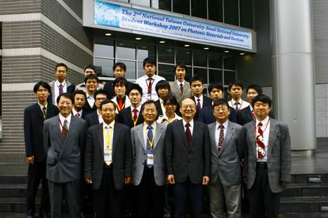
【The 2nd National Taiwan University-Seoul National University Student Workshop 2007 on Photonic Materials and Devices】
November 17th to 21st, 2007
National Taiwan University
Highlights compilation: GIPO Ph.D. candidate Tsung-Yi Tang
The 2nd National Taiwan University-Seoul National University Student Workshop on Photonic Materials and Devices opening ceremony took place on November 19th, and came to a successful conclusion in the afternoon, two days later. This event was first held at Seoul National University last year (2006). After receiving a strongly positive response from both sides last year, workshop was held this year under the leadership of recently appointed GIPO Chairman Sheng-Lung Huang. One major difference, however, was that National Taiwan University was the workshop’s host this year. Thus, participating NTU students were responsible for matters related to the workshop. After experiencing the two-day workshop, I took the first step towards understanding the procedure for hosting such an event. Furthermore, my responsibilities during this workshop allowed me to gain a better understanding of how to compile a workshop handbook. Attending the workshop was an invaluable experience. Thank you to GIPO for hosting such an event. Also, thank you to the professors and staff of National Taiwan University and Seoul National University for promoting and supporting this workshop.
This year, the key subject was photonic materials and devices. 17 papers were presented, of which nine were presented by NTU students and the rest by Seoul National University students. From NTU, the participating students and their professors were as follows: Chen, Mei-Hsin (Professor Wu, Chih-I)、Cheng, Tzu-Huan (Professor Liu, Cheewee)、Wang, Sung-Li (Professor Peng, Lung-Han)、Chang, Chih-Hao (Professor Wu, Chung- Chih)、Chang, Yung-Ting (Professor Lee, Jiun-Haw)、Hsu, Sen-Ming (Professor Chang, Hung-Chun)、Min-Yung Ke (Professor Huang, Jian-Jang)、Hsu, Kuang-Yu (Chairman Huang, Sheng-Lung) and me (Professor Yang, C. C.). NTU participants were all GIPO students. For Seoul National University, most of the participating students were from the Department of Materials Science and Engineering. During this event, I learned for the first time how to arrange the agenda for a conference. Aside from considering the topics of the papers presented, one must also take tours, rest times, and meal times into consideration to maximize the effect of the exchange. The final agenda for the conference was comprised of five sessions: optical characterization and modeling, wide band-gap semiconductors, OLED, infrared optoelectronics, and photonic devices. Among the papers presented at the conference, the paper of Professor Euijoon Yoon’s lab left a special impression with me. The main research subject in his laboratory is gallium nitride materials and the growth of nanostructures, and this subject is closely related to my own research subjects. Aside from learning about each party’s research subjects, the conference also provided us with an opportunity to measure everyone’s ability to use English to present their papers. In terms of English ability, I feel that the Korean students are slightly stronger than us. During rest times and meal times, everyone had a chance to chat and learn about differences in culture and everyday living.
A series of laboratory tours was scheduled for the last day of the conference. Professor C. C. Yang began the proceeding by introducing the Nano Center. Next, Dr. Chen, Li-Chyong introduced the research and equipment in the Center of Condensed Matter Sciences. Last, was a tour of the Nano-Electro-Mechanical-Systems Research Center. During the tours, I couldn’t help comparring all this with what we observed during our visit to Korea. Last year, we toured the ISRC (Inter-university semiconductor research center), and KANC (Korea Advanced Nano Fab Center). Compared with the centers toured this year, the two research centers in Korea integrate a large number of instruments. The LED manufacturing equipment, with purposes ranging from epitaxy to processing and to packaging, is relatively complete. NTU’s Nano Center and the Center of Condensed Matter Sciences are comprised of several laboratories of different research groups. Thus, the equipment contained within is purchased based on the individual need of each laboratory. Each laboratory is small yet compact, able to perform research independently. Conversely, each laboratory is able to focus only on a relatively small range of research. On the whole, I feel the NTU centers lack vertical integration. Also, many restrictions go along with use of the instruments as they belong to different research groups.
During this event, the time we spent with the Korean students allowed us to achieve our goal of cultural and academic exchange. We also learned about the basics of hosting a workshop. Thank you to those who promoted this event, and to each of the participating students for contributing to the success of this workshop.
 |
|
The professors and students of both participating parties. The first row from right to left are Profs. Sheng-Lung Huang, C. C. Yang, Soo-Chang Pei (Dean), Jang-Joo Kim, Euijoon Yoon, Gong-Ru Lin. |
![]() Research Result Column for the Program of
“Aiming for Top University”
Research Result Column for the Program of
“Aiming for Top University”
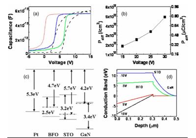
Observation of 394 nm Electroluminescence from Low-Temperature Sputtered n-ZnO/SiO2 Thin Films on top of the p-GaN Heterostructure
Professor JianJang Huang
Graduate Institute of Photonics and Optoelectronics, National Taiwan University
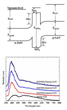
ZnO, with a large direct bandgap of 3.37eV, is a promising material for ultraviolet (UV) light emissions or photo detections. It possesses unique characteristics such as a large exciton binding energy of 60meV (versus 26meV for GaN), easy processing due to amenability to conventional chemical wet etching, and the possibility of low-temperature growth.
In this work, we fabricated an n-ZnO/SiO2/p-GaN light emitting diode with 394nm UV light emission. We compare samples with and without a SiO2 current blocking layer. With a SiO2 layer, EL spectrum shows a sharp emission peak at 394 nm. The 394 nm peak is attributed to the recombination of accumulated carriers between n-ZnO/SiO2 and p-GaN/SiO2 junctions. As for the sample without a SiO2 layer, only the 400-800 nm broad band is observed, which is due to Mg+ deep-level transition in the GaN and defects related recombination in the ZnO layers.
 |
 |
|
(Upper figure) Energy band diagram of n-ZnO/SiO2/p-GaN LEDS. (Lower figure) EL spectra of n-ZnO/SiO2/p-GaN LEDs with different SiO2 thicknesses. The bias current is 20mA. The EL intensity is expressed in linear scale. |
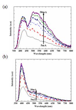
EL spectra of a ZnO-GaN LED (a) and a n-ZnO/SiO2 (3nm) /p-GaN LED (b). The bias current ranges from 5mA to 30mA at a step 5mA. |
![]()
![]()
Analysis of the Inter-Channel Response in a MEMS 1xN2 Wavelength-Selective Switch (WSS)
Professor Jui-che Tsai
Graduate Institute of Photonics and Optoelectronics, National Taiwan University
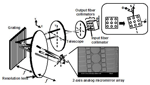
Dynamic wavelength-selective switches (WSS) have been of great interest as they integrate wavelength demultiplexing, switching, and re-multiplexing functions in compact packages. They also enable management of optical networks at the wavelength level and are the building blocks of wavelength-selective crossconnets (WSXC). A wavelength-selective switch can be realized by various distinct techniques, such as the free-space MEMS (micro-electro-mechanical systems) optical system with a tilting-micromirror array, the hybrid PLC (planar lightwave circuit)-MEMS architecture, and liquid crystal-based modules.
Until now, the maximum output port count for a free-space MEMS 1xN WSS with a one-dimensional (1D) collimator array is N = 4. The port count can be increased from N to N2 by using a two-dimensional (2D) collimator array in conjunction with a two-axis beam-steering mechanism. The two-axis beam steering is implemented by either two linear arrays of one-axis analog micromirrors with orthogonal scanning directions, or a monolithic two-axis MEMS scanner array.
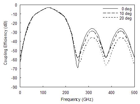
In our previous study of free-space MEMS 1xN2 WSS, we observed a large inter-channel response at a horizontal output port which is aligned with the input along the dispersion direction. The inter-channel response is undoubtedly undesirable for optical communication. It is preferable to suppress the inter-channel response, therefore maximizing the pass and stop bandwidths, allowing for channel misalignment due to laser drift from the ITU grid, and relaxing packaging requirements. We have developed a theoretical model based on Fourier optics and the power-coupling overlap integral. The inter-channel response in a MEMS 1xN2 WSS is investigated and it, according to the simulation results, depends significantly on the output port location and the radius of curvature of the micromirrors. A simple solution is then proposed to suppress the inter-channel response in a 1xN2 WSS. It can be achieved by rotating the 2D collimator array such that no output port is aligned with the input along the dispersion direction. With 20° rotation, 10-dB and 8.2-dB suppressions are demonstrated theoretically and experimentally, respectively, for a prototype system.
|
|
|||
|
Figure 1 Schematic of the 1xN2 wavelength-selective switch (WSS) with a rotated 2D collimator array. A two-axis analog micromirror array is used for 2D beam steering. |
|||
|
|||
|
|
![]()
![]()
A Compact MMI-based Silicon-on-Insulator Polarization Splitter
Professor Ding-wei Huang
Graduate Institute of Photonics and Optoelectronics, National Taiwan University
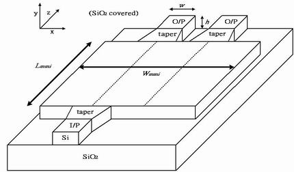
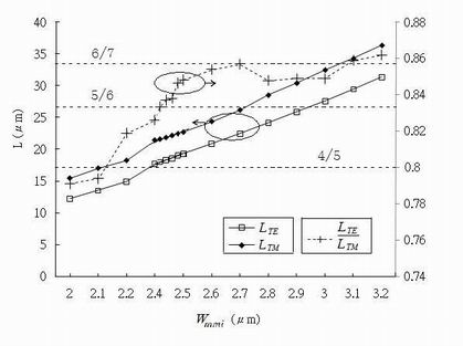
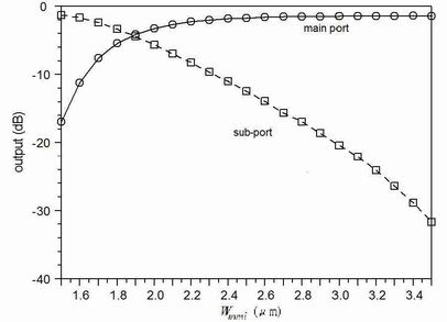
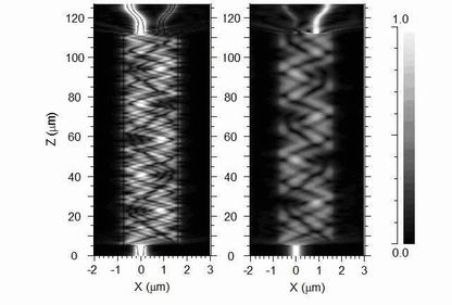
An MMI coupler polarization splitter based on geometrical birefringence is proposed. When the ratio of the self-imaging length of TE mode LTE and the self-imaging length of TM mode LTM equals to the ratio of two consecutive integers m and m +1, i.e., LTE/LTM = 1/2, 2/3, 3/4,…, m/(m +1), meanwhile the length of the MMI device is chosen to satisfy Lmmi = mLTM = (m+1)LTE, then the two modes can be successfully separated into 2 different output ports as shown in Fig. 1. The intersects between horizontal lines and the curve of Wmmi in Fig. 2 are the design solutions, we pick Wmmi as small as possible to achieve the largest difference of the self-image lengths between TE and TM modes and the shortest length of the entire device. Note that when Wmmi is too small, the separated modes may couple to each other between the two output ports. The relation between the output power and Wmmi is shown in Fig. 3. To avoid coupling and make the extinction ratio between the main port and sub-port to achieve -10 dB or more, thus, the length of the polarization splitter is about 107 μm when the width of the MMI is 2.42 μm and the extinction ratio of the two polarization components can achieve -10dB. The polarization splitting behavior is shown in Fig. 4.
 |
|
Fig. 1 Schematic of MMI-based polarization splitter in a SOI channel waveguide include input and output ports, tapers, the MMI waveguide and silica substrate. |
|
|
|
Fig. 2 The self-imaging lengths of TE and TM modes and their ratio, LTE/LTM. The intersects between horizontal lines and the curve of Wmmi are the design solutions. |
|
|
|
Fig. 3 The relation between the output power and Wmmi |
|
|
|
Fig. 4 Polarization splitting behavior in the device. The left-hand side is the result of TE mode and the right-hand side is the result of TM mode |
![]()
![]()
|
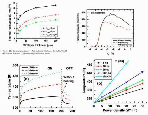
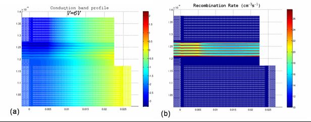
Transient study of self-heating effects in AlGaN/GaN HFETs Professor Yuh-Renn Wu Graduate Institute of Photonics and Optoelectronics, National Taiwan University GaN transistors offer a unique combination of high speed and high power. Devices capable of operating at close to 180 GHz can also be biased so that each electron may emit up to 100 phonons as it transits from source to drain. Therefore, strong heating effects in GaN transistors are expected. Here we present a model combined of the time dependent thermal conduction equation with Poisson and drift-diffusion model to study the relation electron current and temperature in pulsed and DC conditions. The studies show that self-heating effects are significant in high power AlGaN/GaN HFETs even for very short pulse widths (~ a few nanosecond). The results explain part of the reasons for the low velocity observed in the short pulse measurements. Our calculations also suggest that the device performance could improve more than 30 % if we can efficiently remove the self-heating effects. The developed model can be used on studying the power electronic transistor but also the power LEDs circuit. In the future work, we will apply our model in analying the heating effect in power white light LED devices. |
 |
|
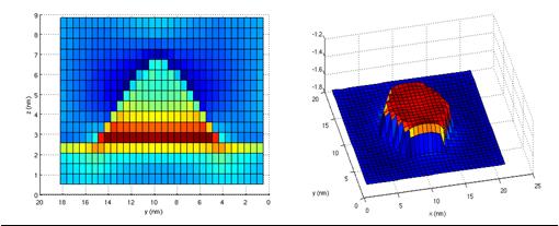
Fig. 2 (a) The simulated channel temperature increase versus time for different output power densities. After 200 ns, the heating source is removed and the temperature decreases rapidly; and (b) the simulated average channel |
![]()
![]()
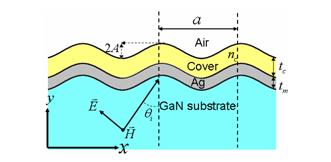
Numerical study on surface plasmon polariton behaviors in periodic metal-dielectric structures using a plane-wave-assisted boundary integral-equation method
Professor Yean-Woei Kiang
Graduate Institute of Photonics and Optoelectronics, National Taiwan University
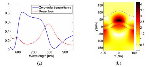
A hybrid technique based on the boundary integral-equation method is proposed for studying the surface plasmon polariton behaviors in two-dimensional periodic structures. Considering the periodicity property of the problem, we use the plane-wave expansion concept and the periodic boundary condition instead of using the periodic Green’s function. The diffraction efficiency can then be readily calculated once the equivalent electric and magnetic currents are solved that avoids invoking the numerical calculation of the radiation integral. The numerical validity is verified with the cases of highly conducting materials and practical metals. Numerical convergence can be easily achieved even in the case of a large incident angle as 80o. Based on the numerical scheme, a metal-dielectric wavy structure is designed for enhancing the transmittance of optical signal through the structure. The excitation of the coupled surface plasmon polaritons for the high transmission is demonstrated.
|
|
|
Fig. 1 Schematic illustration of a wavy layered structure. The grating period is a, and the amplitude of the sinusoidal variation is A. The cover layer, with its thickness denoted by tc, has a refractive index nc. The thickness of the Ag film is tm. |
 |
|
Fig. 2 (a) Zero-order transmittance and power loss versus wavelength. The structure parameters used are a = 218 nm, A = 20 nm, tm = 28 nm, tc = 70 nm, and nc = 2.7. (b) Magnitude distribution of the magnetic field at λ0 = 630 nm. |
|
Associate Professor Prof. Ming-Hua Mao received the B.S.E.E. and M.S.E.E. degrees from National Taiwan University in 1990 and 1992, respectively. After the military duty, he pursued his further study at the Technical University of Berlin in 1995, received the Dr.-Ing. degree, and then joined the faculty of the Department of Electrical Engineering, National Taiwan University in 2000. |
|
|
People are most curious about why he chose Germany for his PhD study. Prof. Mao feels it was a natural choice in stead of a difficult decision. So, when people asked "Why Germany?", he has to think hard for the answer. The thought began with the participation in a high school scientific meeting in Germany in 1986. He was the representative from Taiwan. Back then, it was a rare opportunity to go abroad before one fulfilled his military duty. Through this special event, Prof. Mao acquired an obscure but good impression about Germany. Some of his hobbies are Germany- or german language- related, such as classic music and history. Studying abroad is a golden stage in one's life time to deeply appreciate a certain culture and language. Since English is the first foreign language in most Asian countries, the non-English-speaking countries were considered to the destinations for further study. Germany is famous for the fundamental scientific research. Prof. Mao intended to engage in solid-state research which is more physics-oriented in the whole EE research areas. Therefore, to study in Germany seemed to be a very natural choice either from the professional or from the non-professional point of view. During his stay in Berlin from 1995 to 2000, research on quantum-dot lasers developed vigorously. Back to the year of 1994, Prof. Bimberg's group in the Technical University of Berlin just demonstrated the world's first current-injection quantum-dot laser. Prof. Mao joined this group and investigated the dynamic properties of quantum-dot lasers. After returning to NTU as a faculty member, he continued his research on quantum-dot opto-electronic devices in cooperation with Prof. Hao-Hsiung Lin, and on the other hand, he began to engage in the study of micro-cavities, including photonic crystals and micro-disk structures, to produce micro-cavity lasers. Recently, Prof. Mao's group fabricated successfully a quantum-dot micro-disk laser with Q factor more than 14,000. Prof. Mao is interested in classical music, history, and traveling. He not only visited J. S. Bach's hometown in Eisenach and the nearby Wartburg where Martin Luther translated the Bible into German, but he also witnessed the first-generation electron microscope built in the Technical University of Berlin in the 1930s. All made his heart tremble for the vicinity of these sites where major historical events took place. |
|
|
Optoelectronic Device Simulation Laboratory The research topics of our laboratory are focused on following subjects: Design and Analysis of High Power White Light LEDs: |
|
The nitride based alloys have a wide range of emission spectrum from UV to infrared. Therefore, it is a very good candidate for lighting technologies. As the price of energy continues to increase due to the exhaust of oil, increasing the power consumption efficiency and reducing the waste of power have become an important issue for today's technology. Solid state lighting is the direct conversion of electricity to visible white light using semiconductor materials, which is a very good candidate to save the power consumption. Therefore, how to design a high power and high efficient white light LED is a very important issue for today’s research. As we know the GaN has very strong polarization field which will lead to quantum confined Stark effects and reduce the lighting efficiency. The layer thickness is also limited and leads to efficiency droop effects. Therefore, how to optimize the device performance becomes an important issue. Our laboratory has developed a serious modeling program to analyze the nitride based materials including, one dimensional and two dimensional, thermo-conduction, Poisson, drift-diffusion and Schrödinger solvers. And we are going to develop three dimensional simulation tools to analyze the wired based materials. With these developed programs, we can analyze the effect of carrier transporting, current spreading, device heating, and polarization so that we can further optimize the device performance.
 |
Modeling the Nitrides-based Band Structures of Quantum Well, Quantum Wire, and Quantum Dot
The use of quantum effects in the optoelectronic devices has made the device design with much flexibility. However, it also increases the complexity and difficulties. Therefore how analyze the change of band structure due the polarization, strain, and thermal effects has become a very important issue. To study the band structures of InGaN quantum dot and wire devices, we are developing the valence force field model to study the strain distribution in the quantum dot and quantum wire device. After obtaining the strain information, we calculated the induced piezoelectric polar charge in the low dimensional devices. A three dimensional (3D) Poisson solver was used to calculate the potential variation induced by polar charges. Finally, full bands k·p model was used to study the energy levels and wave function of electron and hole inside the quantum dot device. We are looking into these low dimensional systems to see if they can provide better quantum efficiency or other beneficial effects to improve the device performance.
|
|
Ferroelectric (or Piezoelectric) / Semiconductor Smart FETs
It has been known that most ferroelectric and piezoelectric materials are very sensitive to stress, temperature, and electric field. Therefore, they are very good candidates for sensor, and memory applications. However, due to their poor conductivity, it is hard to directly use it as an electronic device. Semiconductors such as Si, GaAs, and GaN have relatively better crystal quality and higher mobility. Our research goals are focusing to integrate the both advantages of these materials as one smart sensor FETs. In this study, we calculate the optimization of the device structures and collaborate with prof. Ramesh's group in UC Berkeley.
|
|
|
Small Lab The research of He’s group focuses on both understanding the fundamental aspect of low-dimensional charge transport phenomena in semiconductor nanowire structures and employing these properties to create novel functional nanoelectronic devices as an application. The idea central of He’s group to the vision is that by developing and following a common intellectual path – a bottom-up paradigm for nanoscale science and technology – it will be possible to assemble virtually any kind of device or functional nanosystem, ranging from ultra-sensitive light sensors to powerful nanocomputers, and also to explore new areas of science that exist, for example, at the interface between biology and nanotechnology. |
|
Dr. He’s group is currently involving in three major areas: (1) fabrication and characterization of novel low-dimensional photonic nanomaterials, (2) fundamental physical properties of the nanomaterials and design of functional nano-devices (electronics and optoelectronics), and (3) exploration of the communication between biological systems and nanoscale devices. Dr. He has authored over 20 peer reviewed publications, which have been cited over 100 times in the field of nanoscience and nanotechnology.
Please send comments to GIPO_5@cc.ee.ntu.edu.tw.
Copyright
Graduate Institute of Photonics and Optoelectronics, National Taiwan University