Latest News Special Report Research Result Column Profiles Laboratory Descriptions
![]() Welcome to GIEOE, Professors Cheng, I-Chun; Wu, Yuh-Renn; and
He, Jr Hau
Welcome to GIEOE, Professors Cheng, I-Chun; Wu, Yuh-Renn; and
He, Jr Hau
New members have joined the GIEOE faculty! Their academic and professional backgrounds and specialties are as follows:
|
Position |
Name |
Academic Background |
Research Areas and Specialties |
Professional Background |
|
Assistant Professor |
Cheng, I-Chun |
Ph. D., Princeton University |
Flexible optoelectronic devices |
Princeton University, Postdoctoral Research Associate in Electrical Engineering 2004-2007/01 |
|
Assistant Professor |
Wu, Yuh-Renn |
Ph. D., University of Michigan, Ann Arbor,Dept.of Electrical Engineering and Computer Science |
GaN-based optoelectronic devices |
Research Fellow, University of Michigan, Ann Arbor 2006/09~2007/01 |
|
Assistant Professor |
He, Jr Hau |
Ph. D., National Tsing Hua University, Dept. of Materials Science and Engineering |
Nano-material growth |
National Tsing Hua University, Dept. of Materials Science and Engineering, Postdoctoral Fellow 2005/10~2006/06 Georgia Tech. Postdoctoral Fellow 2006/06~2007/01 |
![]() GIEOE academic visiting highlights
GIEOE academic visiting highlights
|
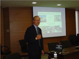
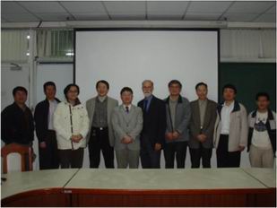
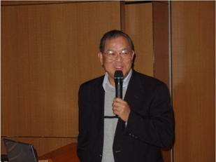
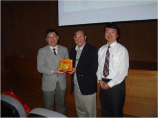
Activity: “Photonics Speech” Time: December 6th, 2 pm. Speaker: Professor John E. Bowers (ECE Department University of California, Santa Barbara) Topic: Silicon Evanescent Photonic Integrated Circuits Professor John E. Bowers visited GIEOE on December 6th, 2006, and delivered the speech “Silicon Evanescent Photonic Integrated Circuits”. GIEOE professors and students attended with enthusiasm. |
|
 |
 |
|
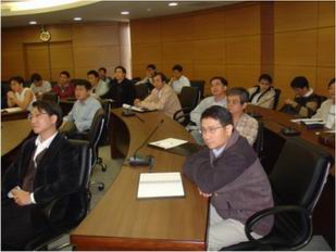
Activity: “OSA-related Issues and Photonics Research and Education” Workshop Time: December 18th, 3:30 pm Speaker: Professor Eric Van Stryland (President of Optical Society of America) On December 18th, 2006 (Monday), OSA president, Prof. Eric Van Stryland visited GIEOE and led the workshop “OSA-related Issues and Photonics Research and Education”. Numerous professors and students attended the workshop and participated in the discussion with enthusiasm. |
|
 |
 |
|
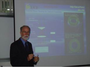
Activity: “The Photonics Forum” Time: December 22nd, 4:30pm Speaker: Prof. Chi H. Lee (University of Maryland, College Park, U.S.A.) Topic: Polymer Photonics Professor Chi H. Lee visited GIEOE on December 22nd, 2006, and delivered the speech “Polymer Photonics”. Professor Lee is humorous and affable, and his speech captivated attending professors and students. Everyone participated with enthusiasm and gained new insights. |
|
 |
 |
![]() Program for
Graduate Students Exchange
Program for
Graduate Students Exchange
between National Taiwan University and Seoul National University
![]()
【The 1st National Taiwan University-Seoul National University
Graduate Student Workshop on Photonic Materials and Devices】
November 19th to 24th, 2006
Seoul National University, Korea
Highlight Compilation: GIEOE Ph.D. candidate Hao-Wu Lin
The 1st National Taiwan University-Seoul National University Graduate Student Workshop on Photonic Materials and Devices took place on November 19th to 24th, 2006 at Seoul National University. It was the first time that both parties had held a workshop of this kind, and placed its focus on graduate students. We arranged the manner in which the workshop proceeded, and both parties appointed representatives as session presiders. Speakers were also mainly graduate students.
Throughout the conference, participating professors and students from Seoul National University extended the warmest hospitality to us. We appreciated their careful and attentive consideration in arranging transportation, meals and conference planning. During our conversations outside conference time, they shared their views and experiences without reservation. Topics of conversation ranged from research topics, to language, culture, history, politics, religion, economics, food, transportation, and much more. Through these exchanges, we’ve come to realize that although we grew up from different backgrounds, our goals and values are not dissimilar.
The topical subjects of the workshop can be roughly divided into six categories: 1) nitride growth, measurement, and analysis; 2) nanostructure growth, measurement, and analysis; 3) light-emitting devices; 4) organic light-emitting diode; 5) waveguide and nonlinear optics; 6) InGaN semiconductors. Each speaker gave a thirty minute oral presentation introducing his/her laboratory and personal research topics. For most of the graduate students of both parties, it was their first time giving a speech of such length in English. Aside from describing our own research accomplishments, we also briefly summarized the research direction and contributions of our laboratory. Everyone prepared and delivered their speech with care and effort.
Following the conclusion of the conference, we were given a tour of Korean large-scale laboratories, including Seoul National University’s ISRC (Inter-university Semiconductor Research Center), and KANC (Korea Advanced Nano Fab Center) located on the outskirts of Seoul. The visit allowed us to experience firsthand Korea’s research environment and attitude.
In preparing for the conference, everyone was nervous and excited. However, the meeting was quite successful. After four days of academic reflection, cultural and linguistic shock, we happily returned to Taiwan feeling fulfilled and knowing that we had taken a first step in internationalization.
We have three professors to thank for the successful completion of this exchange: GIEOE Chairman C. C. Yang, Vice Chairman Sheng-Lung Huang, and Professor Yun-Li Li painstakingly accompanied and guided us throughout the conference. In addition, our student group leader Cheng-Yen Chen and GIEOE staffer Ms. Hsiao-Wen Lin spent much time and effort in preparations for this trip. Furthermore, the financial assistance from NTU was crucial to the actualization of the trip. Although it was the first exchange, I believe that this activity is quite meaningful for Taiwan’s graduate students. This exchange proved more of a challenge for our brainpower and communication skills and more of a learning experience than the ordinary international conference. I hope that this kind of activities can be continued in the years to come. I believe that my fellow students who continue to participate will also find the exchange fulfilling.
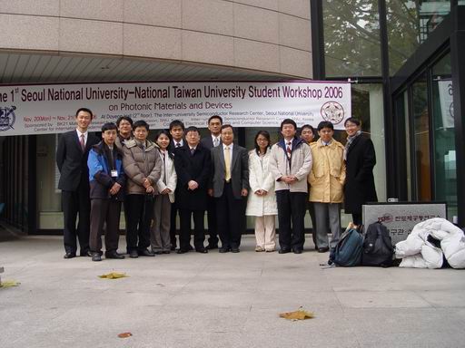 |
| Professors and graduate students representing NTU with Korean hosting professor, Prof. Euijoon Yoon |
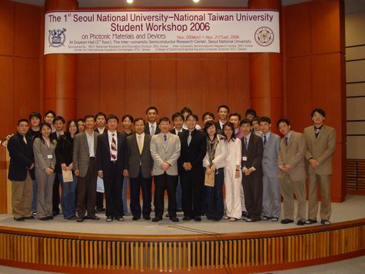 |
| Participating professors and students of both parties in the conference room |
![]() “Agreement
on Student Exchange
“Agreement
on Student Exchange
between College of Engineering, Seoul National University
and College of Engineering & College of Electrical Engineering and Computer Science,
National Taiwan University” signed
![]()
January 15th, 2007
NTU, College of EECS, Barry Lam Hall, 7F Conference Room)
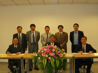
To promote academic exchange and cooperation, NTU’s College of Engineering and College of EECS and Seoul National University’s College of Engineering signed an agreement to finalize the student exchange program. The agreement specifies the period of time, number of students exchanged, and related details. This opened a new chapter in the cooperative exchange between both parties.
The ceremony took place at 11 a.m. at NTU’s Barry Lam Hall in the 7th floor conference room. Professor Doh-Yeon Kim(Department of Materials Science and Engineering, Dean of the College of Engineering), Professor Woojae Seong(Department of Ocean Engineering, Associate Dean for International Affairs, College of Engineering), and Professor Euijoon Yoon(Department of Materials Science and Engineering)represented Seoul National University. Professor Huan-Jang Keh (Dean of College of Engineering, National Taiwan University), and Professor Soo-Chang Pei (Dean of College of Electrical Engineering and Computer Science, National Taiwan University) represented National Taiwan University. Both parties signed the agreement.
The participating professors of NTU also included Professor Ming Ouhyoung (Vice Dean of EECS), Professor C. C. Yang (Chairman of GIEOE), Professor Horn-Jiunn Sheen (Professor of Institute of Applied Mechanics), Professor Yun-Li Li (Professor of GIEOE). During the briefing before the ceremony, Deans of NTU’s College of Engineering, College of EECS, and Seoul National University’s College of Engineering provided introductions in sequence to increase mutual understanding. Next, both parties signed Chinese and English versions of the agreement.
 |
|
Representatives of both parties during the signing ceremony. Front row from the left: Dean Soo-Chang Pei, Dean Doh-Yeon Kim, Dean Huan-Jang Keh; back row from the left: Prof. Euijoon Yoon, Prof. Woojae Seong, Chairman C. C. Yang, Vice Dean Ming Ouhyoung, Prof. Yun-Li Li |
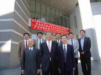
In addition, GIEOE, NTU and Department of Materials Science and Engineering, College of Engineering, Seoul National University signed a Memorandum of Understanding on Academic Exchange, outlining the annual graduate students exchange workshop conducted by both parties. GIEOE, NTU and Department of Materials Science and Engineering, Seoul National University already successfully held the 1st Graduate Student Workshop on Photonic Materials and Devices near the end of November. We anticipate that the signing of this agreement will lay a solid foundation of cooperation for the upcoming workshop.
 |
|
Representatives of both parties in front of Barry Lam Hall. Front row from the left: Dean Soo-Chang Pei, Dean Doh-Yeon Kim, Dean Huan-Jang Keh; back row from the left: Vice Dean Ming Ouhyoung, Prof. Woojae Seong, Prof. Euijoon Yoon, Chairman C. C. Yang, Prof. Yun-Li Li |
![]() Research Result Column for the Program of
“Aiming for Top University”
Research Result Column for the Program of
“Aiming for Top University”
Phosphor-free, all-InGaN/GaN quantum-well white-light light-emitting diode of stable spectrum and almost ideal CIE chromaticity condition
Professor C. C. Yang’s Group
Graduate Institute of Electro-Optical Engineering, National Taiwan University
(e-mail) ccy@cc.ee.ntu.edu.tw
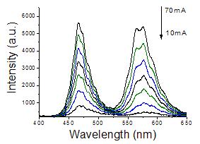
We successfully fabricate a white-light InGaN/GaN quantum-well (QW) light-emitting diode (LED) with its electroluminescence spectrum close to the ideal condition in Commission International de l'Eclairage (CIE) chromaticity. The epitaxial structure is grown with a special technique of metalorganic chemical vapor deposition. The special growth technique leads to the efficient yellow emission from a few high-indium InGaN/GaN QWs. The color mixing for white light is implemented by adding a blue-emitting QW at the top of the yellow-emitting QWs. The blue shifts of the blue and yellow spectral peaks of the generated electroluminescence spectra are only 1.67 and 8 nm, respectively, when the injection current increases from 10 to 70 mA. Such small blue shifts imply that the piezoelectric fields in our QWs are significantly weaker than those previously reported. This result represents the fabrication of the first phosphor-free white-light LED of almost ideal CIE chromaticity condition in the world. Use of phosphor in fabricating white-light LED has the disadvantages of lower efficiency and lower reliability. This accomplishment should be useful for the developments of solid-state lighting and display.
 |
|
Fig. 1 LED output spectra at various injection current levels. |
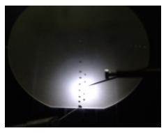 |
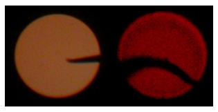
| Fig. 2 Picture of a two-inch epitaxial wafer with a portion excited with 20 mA current. |
![]()
![]()
A CO2 Laser RTA SiOx Based MOSLED
Professor Gong-Ru Lin’s Group
Graduate Institute of Electro-Optical Engineering, National Taiwan University
(e-mail) grlin@ntu.edu.tw
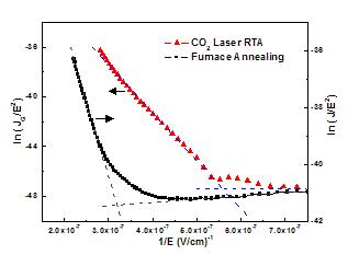
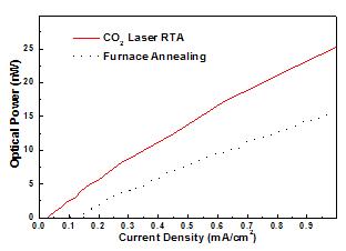
Enhanced near-infrared electroluminescence (EL) of a metal-oxide-semiconductor light emitting diode (MOSLED) made on CO2 laser-annealed SiOx film is demonstrated. The CO2 laser rapid-thermal-annealing (RTA) at an optimized intensity of 6 kW/cm2 for 1 ms assists the synthesis of nc-Si within plasma-enhanced chemical vapor deposition-grown SiO1.25 film. The oxygen-related defects accompanied with the laser RTA process are capable of improving the Fowler-Nordheim tunneling mechanism, which essentially helps carrier injection through the barrier at metal and oxide interface. In comparison with the sample prepared by conventional furnace annealing, the CO2 laser RTA induced defects effectively reduce the tunneling threshold from 3.2 to 1.8 MV/cm. To date, an output EL power of nearly 50 nW from ITO/CO2 laser RTA SiOx/p-Si/Al MOSLED under a biased voltage of 85 V and current density of 2.3 mA/cm2 is preliminarily reported.
 |
 |
|
Fig. 4. Plot of ln(JG/E2) as a function of 1/E for CO2 laser-annealed and furnace-annealed MOSLEDs. |
Fig. 5. P-I curve of the furnace and CO2 laser annealed SiOx based MOSLEDs. |
 |
 |
|
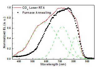
Fig. 7. EL spectra of MOSLEDs made by CO2 laser RTA (line) and furnace-annealed (square) SiOx with decomposed curves at 590, 715 and 810 nm (dashed). |
Fig. 8. Far-field EL patterns of CO2 laser RTA (left) and furnace-annealed (right) MOSLEDs. |
|
|
Professor 1. Background Prof. Liu was born in Taipei, Taiwan, 1963. He received both the B.S. and M.S. degree in electrical engineering from National Taiwan University in 1985 and 1987, |
|
respectively. He received the Ph.D. degree in electrical engineering from Princeton University in 1994. He was with the Department of Electrical Engineering, National Chung-Hsing University in 1994-95. He has joined the Department of Electrical Engineering, National Taiwan University as an Associate Professor since 1996. In 2001, he became a full Professor. Prof. Liu also led a SiGe project in ERSO/ITRI through a special arrangement between NTU and ITRI as a research director with the rank of senior full researcher from 2001 to 2005. 2. Research fields The research in Prof. Chee Wee Liu’s group is based on the SiGe:C and strained Si/high-K/metat gate, including (1) CMOS and Bipolar circuit design using (strained) Si CMOS and Si/SiGe:C HBTs; (2) device modeling and simulation on Strained Si/Ge FET, HBT, and optoelectronics devices; (3) CMOS optoelectronics with detector, emitter and waveguide; (4) material technologies such as SOI, GeOI, SSDOI, smart-cut, buckling quantum wells, nano-mechanics, and strained-SiGe:C; and (5) the rapid thermal processors for RTA, RTO, RTCVD, and wafer bonding. The strained Si/high-K/metal gate is intentionally to bypass the red brick wall on the ITRS roadmap, but the novel applications such as optoelectronics application are also focused. To lower the cost of strained Si technology, special local strain (process strain) technologies are being developed with calibrated process simulation.
3. Honors
4. Habit Go jogging 5. Visions The Si CMOS has market size of ~200B USD in 2004. Without killer applications, it will be difficult to further increase its market size. The display has ~40B USD market size. Si can increase its market size by replacing the current technologies used in the display. The low cost and mature Si technologies can hopefully make LED display to outperform the TFT-LCD in the display market. The indirect bandgap of Si and Ge makes the light emission from Si or Ge to be very inefficient (efficiency far less than a percent), and the bandgap of Si and Ge also limits the emission wavelength to infrared region (1.1 to 2mm). We have tried very hard in the past decade to pump out the visible light from bulk Si by creating the hot electron/hot hole radiative recombination with the photon energy in the visible light range. Note that the switching speed of bulk Si MOS LED was around the order of ms, according to our previous results. This speed is sufficient for display applications. The quantum confinement of Si(Ge) nanocrystallite can have theoretical life time of ns. The III-V LED (light emitting diode) display is limited by cost and size and only has niche applications of the display market. The direct bandgap engineering and nanocrystallite Ge(Si) can potentially tune the emission wavelength into visible wavelength, and can increase the light emission efficiency to ~10%. The ms speed of MOSLED is sufficient for display applications. Due to the emission location from the nanocrystllite embedded in the oxide of the MOS LED. The Si wafer is not necessary and a metal-anode/oxide with embedded nanocrystallite /metal-cathode (MIM LED) is proposed to inject carriers from Schottky barriers. This MIM LED can be potentially fabricated on glass substrate with the size comparable with TFTLCD. This technology will enable Si to share the display markets with TFTLCD technology. |
|

|
Professor Prof. Hao-Hsiung Lin received his B.S., M. S. and Ph. D. degrees from the Department of Electrical Engineering, National Taiwan University in 1978, 1980, and 1985, respectively. Since 1980, he has been with the Department of Electrical |
|
|
Engineering, National Taiwan University.. In 1992, he became a full Professor. He is also with the Graduate Institute of Electronics Engineering and Graduate Institute of Electro-Optical Engineering. His research expertise is in the field of molecular beam epitaxial growth and compound semiconductors. The research in Prof. Hao-Hsiung Lin’s group includes (1) Dilute nitrides: Current work is concentrated on the growth of GaAsSbN lattice-matched to GaAs substrates by gas-source molecular beam epitaxy with RF plasma source. The lowest energy gap of the alloy achieved is ~0.85 eV. This material is promising for GaAs-based long wavelength photodetectors, lasers and tandem solar cells in the future. (2) GaAsSb/GaAs type-II quantum wells: The feature of type-II quantum well is that its transition energy can be less than the fundamental energy gaps of well and barrier. GaAsSb/GaAs lasers with emission wavelength ~1,300 nm have been demonstrated. Current effort is placed on the growth of the GaAsSb/GaAs quantum wells on high index GaAs substrates. (3) InAs quantum dots: Self-assembled InAs quantum dot on GaAs is an important nanostructure for long wavelength GaAs-based lasers. The research is focused on the capping layer (or strain-reducing layer) overgrown on InAs quantum dots. Previous studies on InGaAs capping layer have successfully achieved 1,300 nm lasers. Currently, quantum dots with Sb containing capping layer are studied for extending the emission wavelength. (4) Mid-infrared (MIR) semiconductors: The research is on the molecular beam epitaxial growth of quantum wells for 3–5 mm mid-infrared devices. A room temperature operating InAsSb/InAs quantum well LED was recently demonstrated through a international collaboration work with Lancaster University, UK. Current effect is on the growth of InAlAsPSb/InAsSb quantum well and InAsSb quantum dots on InAs substrates. The structures are promising for the compact, low cost and high efficient mid-infrared light source in the future. |
|
|
|
Professor Professor Yean-Woei Kiang received the B.S.E.E., M.S.E.E., and Ph.D. degrees in 1977, 1979, and 1984, respectively, all from National Taiwan University. From 1982 to 1984, he was a Visiting Scholar at the Department of Electrical Engineering, University of Illinois, Urbana-Champaign, Illinois, U.S.A. In 1979 he joined the faculty of the Department of Electrical Engineering, |
|
National Taiwan University, where he is now a Professor. He has also been a professor at the Graduate Institute of Communication Engineering and the Graduate Institute of Electro-Optical Engineering since 1997 and 2002, respectively. Professor Kiang began his research from the theoretical investigation on electromagnetic wave propagation in random media, electromagnetic wave scattering from inhomogeneous media, and electromagnetic inverse scattering. About ten years ago, he switched the research interest to the electro-optics area focusing on electromagnetic simulation of electro-optical devices. Numerical methods were used to solve the Maxwell equations and related physical or material equations. Either linear or nonlinear phenomena of passive and active electro-optical devices were analyzed. Physical mechanisms were explored for design reference. Professor Kiang has collaborated with Professors C. C. Yang and J. H. Lee for many years. Past research results include analyses of nonlinear coupling effect in semiconductor optical amplifiers, colliding-pulse mode-locking mechanism for semiconductor lasers, performance of semiconductor nonlinear optical loop mirrors, mode coupling effects in fiber gratings, and radiation characteristics of organic light-emitting diodes. He also used the Monte Carlo method in simulating near-IR light propagation and scattering in turbid media to develop applications in optical imaging of biological tissues. Recently, he has been interested in theoretical simulation of photonic crystals and surface plasma waves. Professor Kiang is fond of reading literary works, enjoying the art of Chinese calligraphy, and listening to the classical music (especially the classical guitar). He likes the sea for its immensity and profundity, rage and serenity. Together with his daughters, he is used to collecting the sea shells and studying the wonderful mollusks. Finally, he would like to quote an interesting saying of Newton as follows: To myself I seem to have been only like a boy playing on the seashore, and diverting myself in now and then finding a smoother pebble or a prettier shell than ordinary, whilst the great ocean of truth lay all undiscovered before me. |
|
|
Solid State Lighting and Transparent Transistor Lab Research areas: High Efficiency Light Emitting Diodes, Nano-structure Optoelectronics, Organic and Metal Oxide Transistors, Flexible Transistors and Circuits |
|
1. High performance LEDs
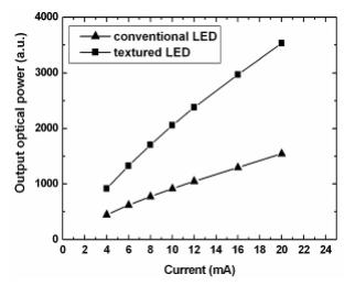
We roughen the LED surface with a novel nano-structure technique. The improvement of light extraction efficiency of a GaN LED can be as high as 2.8 times.
 |
2. Nearly white light emission from GaN based LEDs integrated with SiO2 nanocrystals.
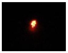
We develop a nearly white light emitting device by integrating blue/green emission from a GaN based LED with red emission from a porous SiO2 layer. The porous SiO2 layer was fabricated by a novel process procedure to create Si nanocrystals on top of the n-type GaN layer. Red light is generated from the metal-oxide-semiconductor (Ni/Au–SiO2 oxide-n-type GaN) structure due to the electron-hole recombination in the Si nanocrystals. The device shows a blue light emission at a low biased voltage and nearly white light emission (green and red colors) at a bias voltage between 14V and 16V. Our results show the potential of applying such an integrated structure to white light illumination.
 |
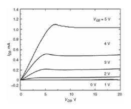
3. High current level, high mobility ZnO TFTs
We demonstrate a high-performance enhancement-mode ZnO TFT on a glass
substrate. The ZnO thin film is deposited by RF magnetron sputtering with
the presence of O2 at low deposition rate and low temperature.
The IDS is as high as 1 mA when biased at the saturation region VDS
= 10-20 V and VGS = 5 V without any post thermal anneal. The Ion/Ioff
ratio is ![]() . We believe the results are among the best ZnO TFTs ever
obtained.
. We believe the results are among the best ZnO TFTs ever
obtained.
 |
 |
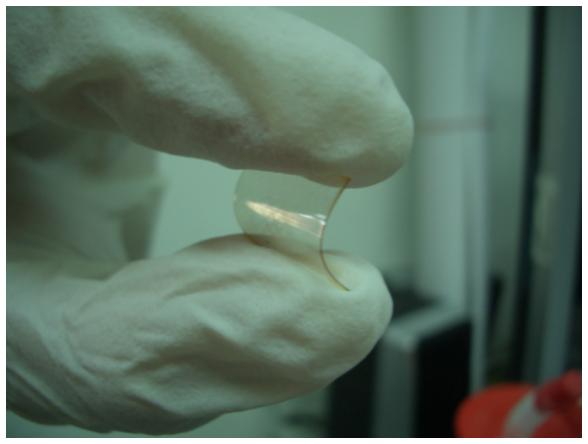
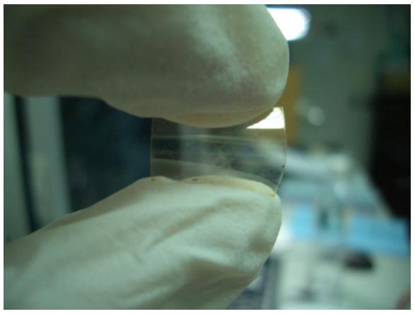
4. Flexible ZnO-based Transparent TFTs
We demonstrate a high-performance top-gate ZnO TFT fabricated on a flexible polymer substrate at low temperature. The ZnO thin film is deposited by RF magnetron sputtering at low deposition rate and low temperature. All the patterns are defined by standard photolithography. The IDS, without any contact alloy, is as high as 0.5mA under a bias condition VGS=0V and VDS=10-15V with a TFT gate size W/L=600μm /300μm. The average optical transmission of the entire TFT structure in the visible range of the spectrum is about 82% while the transmission at 550 nm is 88%.
 |
 |
5. DC and AC Characterization of Organic TFTs
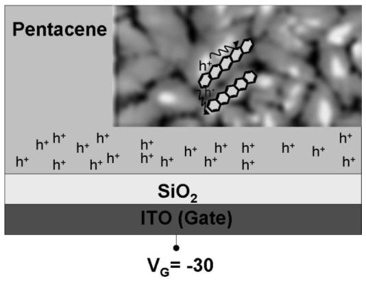
We collaborate with ITRI to build up both AC and DC models for pentacene TFTs. We also analyze quasi static C-V profiles of such a device. The endeavor has lead to a carrier transport model that explains the carrier behavior in an organic transistor.
 |
|
Analysis and Design of Photonic and Optoelectronic Devices With the progress of computer hardware today bringing about the capability for more complicated and massive computation structures, we are able to “foresee” the result via simulation before conducting the experiment. Founded in 2003 and located at Room 351B on the third floor of College of Electrical Engineering and Computer Science, Photonics Simulation |
|
Laboratory is dedicated to treating photonic phenomena with various numerical methods. The equipment consists mainly of several servers, personal computers and a small-scale computer cluster. Although there are quite a few commercial software suites that can assist in the research, their ranges of application do have limits; to accommodate to research subjects of the many directions, the laboratory mainly composes simulation tools using programming languages such as MATLAB and C/C++. The major research subjects in recent years are as follows:
Photonics and applications of photonic crystals and nanostructures: Analysis of the band structures of dispersive and nondispersive as well as lossy and lossless materials, for designing slow-light structures, nonlinear optical switches, communication devices, etc.
Analysis and design of displays and light-emitting devices: Enhancement of emission efficiency by means of periodic and aperiodic photonic structures.
Analysis and design of solar cells: Enhancement of light-coupling efficiency by means of periodic and aperiodic photonic structures, and analysis of electrical properties.
Analysis and design of optical communications and integrated optics: Design of wavelength division multiplexers and analysis of transmission characteristics of optical signals in optical fibers, under different modulations (e.g. OFDM).
Electromagnetic characteristics of metamaterials and left-handed materials: Study of electromagnetic characteristics and phenomena of metallic microstructures, such as the Reverse Doppler Effect.
Improvement of photonic and electromagnetic simulation techniques and development of new methods: Development or improvement of methods of analysis in light of the above problems. Currently applied are the methods of plane-wave expansion, finite-difference frequency-domain, finite-difference time-domain, and so on, utilizing specific hardware (graphic card and FPGA) to accelerate the computation in the mean time.
The research of the laboratory concentrates on the model construction, numerical analysis, and design application of photonic and electromagnetic study. It is hoped that our research would be able to provide study of related fields with clearer understanding on the theory, thereby reaching goals more readily. Therefore by continuously improving and developing related techniques, become a leader in this area, and apply the techniques to emerging and fascinating realms of photonics and electromagnetics as well as the industry of optoelectronic technology; by mutual cooperation with experiments and practical problems, probe into and analyze the reason behind the phenomenon, and then derive possibly applicable or useful designs. In the long run we wish to lower the cost and shorten the time of implementation through theoretical analysis and numerical computation, accomplishing the mission of “contributing our specialty to the academia and the industry by employing our abilities of theoretical analysis and numerical computation in the fields of photonics and electromagnetics”.
|
Micro Optics Laboratory 1. Overview The research fields of Micro Optics Laboratory includes 1. Optical Micro-Electro-Mechanical Systems (Optical MEMS) 2. Display Technology: Micro Imprinting Technologies for Micro Lenses |
|
3. Optical Communication Components- Optical Switches and Variable Optical Attenuator
4. Display Vacuum Panels Research
5. MEMS Bio-sensors for Carbon-dioxide Gas
In terms of physical space, The Micro-Optics Laboratory can be divided into two areas: optical design area and optical component measurement area. The optical design area has three high- speed dual-core LINUX workstations for simulating and calculating traditional optical lenses and diffractive optical components. In addition, we have a large capacity file server for storing and auto-backing up the simulation and calculation results. We also have licensed commercial simulation software such as ZEMAX, TRACEPRO and OSLO, and we also develop our own optical simulation software for lens design. On the other hand, the optical component measurement area has a floating optical table, storage shelf over optical table, red and infrared laser source, beam profiler, power meter, double-row ball bearing linear stages, DC power supply, full color CCD monitor, two 3-D microscope and an image processing PC, which are perfectly suitable for measuring micro-scale optical elements.
The present research topics include: (1) Manufacturing VOA and optical switch using MEMS technology; (2) Infrared ray vacuum measurement system; (3) Application of surface plasma to solar cells and organic membranes.
2. Research Topics
(1) Optical Switches
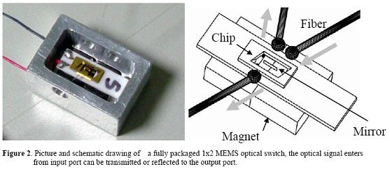
Our laboratory successfully designs and fabricates 2-D MEMS (Microelectromechanical systems) optical switches. Microelectromechanical Systems generally range in size from a micrometer to a millimeter. At these size scales, the standard constructs of classical physics do not always hold true. Due to MEMS’ large surface area to volume ratio, surface effects such as electrostatics and wetting dominate volume effects such as inertia or thermal mass. They are fabricated using modified semiconductor fabrication technology (used to make electronics), molding and plating, wet etching (KOH, TMAH) and dry etching (RIE and DRIE), electro discharge machining (EDM), and other technologies capable of manufacturing very small devices. We use MEMS technology as sputter, wet etching, dry etching, and photo lithography to manufacture optical switch. With accurate design and measurement, our group report electromagnetically actuated two-dimensional micro electromechanical systems optical switches. The operating voltage is less than 1 volt in our system and could be precisely used in WDM (wavelength-division multiplexing) system. We publish our result in Proc. of SPIE, Journal of Light Wave Technology and international conference. The pictures below are our result and design idea.
 |
(2) Variable Optical Attenuator
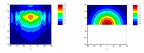
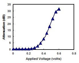
The VOA (Variable optical attenuator) is used to reduce the light power and control the power equalization of different channels in the wavelength division multiplexing (WDM) system. In addition to fast response time, the MEMS VOA provides large range of attenuation and high performance. We present the design and test of a MEMS VOA without complicating circuit made by low-cost wet-chemical etching micromachining processes on silicon wafers. The actuation voltage is less than 0.6 volt due to large electro-magnetic force and the dynamic range is up to 30 dB. The device can be easily configured into normally-on or normally-off modes by changing optical packaging configurations. The two pictures below are the testing result of published paper. The first picture is the off-on state power spectrum of VOA. The second picture is attenuation versus applied voltage.
 |
 |
(3) Display Vacuum Panels Research
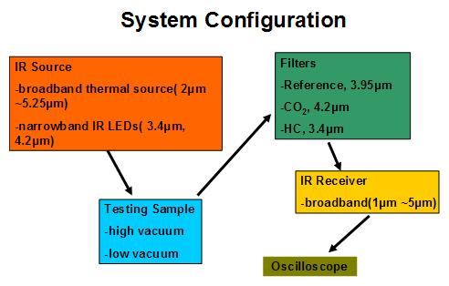
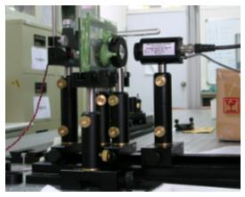
FED (Field emission display) is a potential display technology of next generation with better image quality than liquid crystal display and lower production cost. The goal of our research is to design an innovating vacuum panel measurement to improve the nowadays research of FED and reduce the cost of mass production. Our laboratory reports the non-invading infrared ray system to focus on the variety and concentration of vapor, then try to use these data to deduce the pressure of the vacuum. We substantially increase the accuracy of FED panel by improving our optical system many times. Moreover, we can find the signal of low-pressure vacuum is much lowered than high-pressure vacuum. The picture below is our system configuration.
 |
 |
(4) Organic Membrane Studies
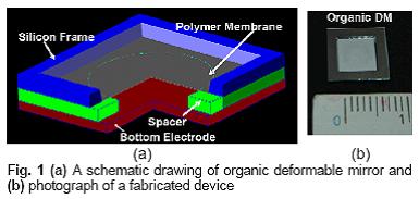
Organic polymer membrane can be used as deformable mirrors that can be incorporated into the optical design to change optical magnification without macroscopic moving parts. In our system, the fabricated device has optical power of 30-diopter that is two orders of magnitude higher than commercially available device. The surface roughness of the organic membrane is measure to be less than 15 nm, corresponding to less than λ/20 in the visible light range. With curve fitting, we found the actuated membrane is close to parabolic shape which has less aberration than spherical lens and therefore is suitable for imaging systems.
 |
(5) LED Package Design Research
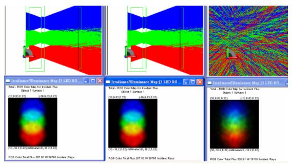
LED (Light emitting diode) technology is a very important compnent in nowadays Taiwan’s industry. The high power and white LED will be applied in our lives in near future. We use optical simulation software TRCAEPRO and thermal simulation software FLUNT to simulate the packaging design of massive LED array in our laboratory. We change and diffuse the propagating direction of the light to reach the uniformity of the white light with redesigned micro-lenses. In thermodynamics part, the simulation software ANSYS is used for understanding the initial mechanical structure of LED. And the thermodynamic and fluid dynamic system is simulated by FLUNT. The pictures below are our simulation result.
|
|
Please send any comment to eoe5@cc.ee.ntu.edu.tw
Copyright
Graduate Institute of Electro-Optical Engineering, National Taiwan University