|
Efficiency Enhancement of Photon Color Conversion from an InGaN/GaN Quantum Well into a Colloidal Quantum Dot Located in a Metal Nanotube
Professor C. C. Yang's Laboratory
Graduate Institute of Photonics and Optoelectronics, National Taiwan University
台湾大学光电所 杨志忠教授
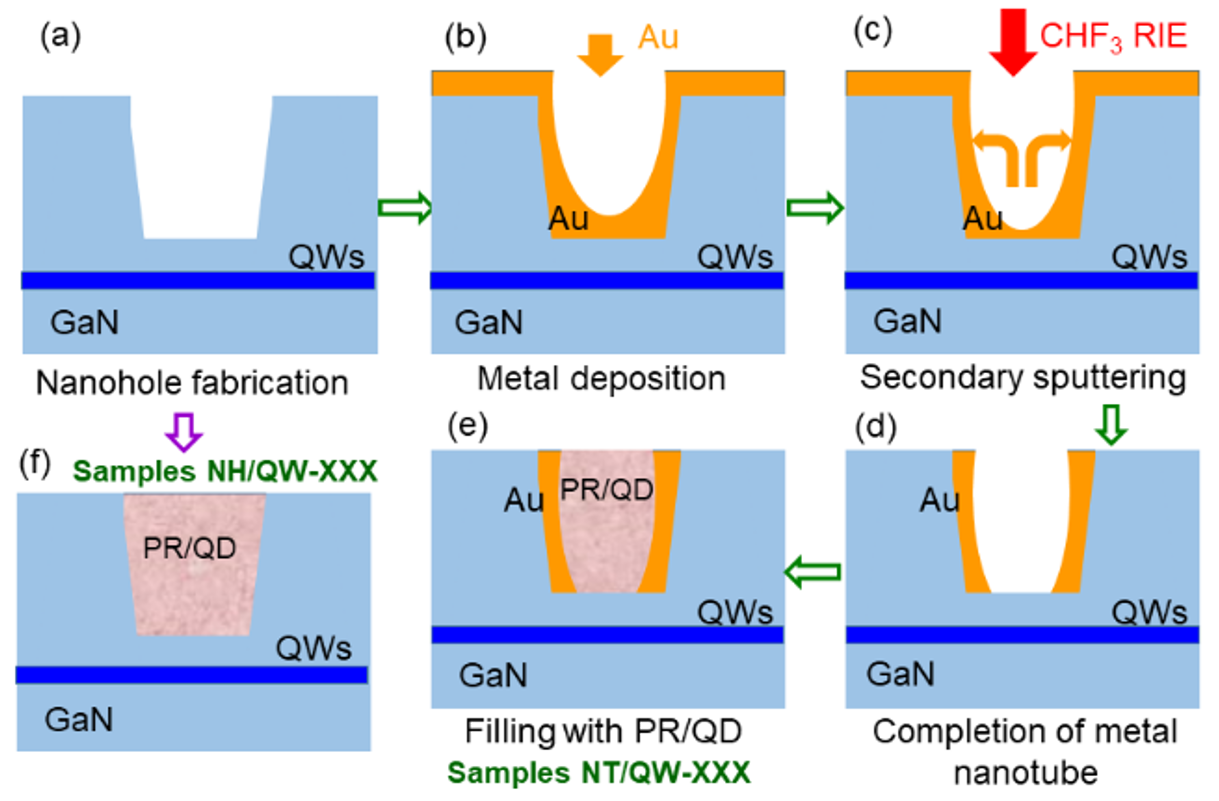
For implementing a surface plasmon (SP) coupling effect to enhance the efficiency of the color conversion from a blue-emitting InGaN/GaN quantum well (QW) into green- and red-emitting colloidal quantum dots (QDs), an Au sidewall layer is fabricated in a surface nanohole (NH) on a QW template to form an Au nanotube (NT) structure for accommodating the inserted QDs. The Au sidewall layer is implemented through Au deposition, followed by a secondary sputtering process in a reactive ion etching chamber. The enhanced efficiency of the Förster resonance energy transfer (FRET) from the underlying QW structure into the inserted QDs is observed, when compared with the result of a surface NH sample without Au sidewall layer. Meanwhile, with a QD inserted into an Au NT, its emission efficiency is increased, when compared to that of a QD inserted into a GaN surface NH. Those efficiency increases are caused by the SP coupling effect of the Au sidewall layer. The combined effect of the efficiency increases of FRET and QD emission leads to an enhanced color conversion process. Figures 1(a)-1(e) show the procedures for fabricating a metal nanotube (NT/QW-XXX) sample. Figure 1(f) shows the structure of a nanohole (NH/QW-XXX) sample. Figure 2 shows the TEM image of an NT/QW-XXX sample after the RIE secondary sputtering process. Here, the dark regions inside the NH correspond to the Au distribution. Table 1 shows the data of PL decay time, IQE, and FRET efficiency in various NT/QW-XXX samples, including the insertions of green QD (GQD), red QD (RQD), GQD plus RQD (GQD+RQD), and pure photoresist (PR).
|

|

|
|
Fig. 1. (a)-(e): Schematic illustrations of the procedures for fabricating an NT/QW-XXX sample. (f): Schematic illustration of the structure of an NH/QW-XXX sample.
|
Fig. 2. Cross-sectional TEM image of an NT/QW-XXX sample after the RIE secondary sputtering process.
|
|

|
|
Table 1. PL decay times of QW, GQD, and RQD emissions in those NT samples with Au sidewall layers fabricated on the QW template. The numbers inside the parentheses (curly brackets) show the QW IQEs at different fabrication stages (the FRET efficiencies from QW into QD).
|
Quasi-van der Waals epitaxy of Bi on (111) Si
Professor Hao-Hsiung Lin's Laboratory
Graduate Institute of Photonics and Optoelectronics, National Taiwan University
台湾大学光电所 林浩雄教授
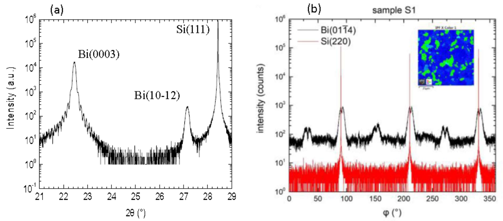
Bi is a nontrivial semimetal, with tiny negative bulk band gap and very small effective mass in certain orientations, allowing the band structure be transferred to semiconductor through quantum size effect. Because of the strong spin-orbit interaction, its surface states split into two bands with a gap of 0.8 eV, which makes it also a promising material for spintronics. In this work, Bi thin films were grown on (111) Si using MBE, and characterized using XRD, TEM, and EBSD. All the Bi films are highly (0003) textured and contain two twinning domains. The basic lattice parameters c and
a
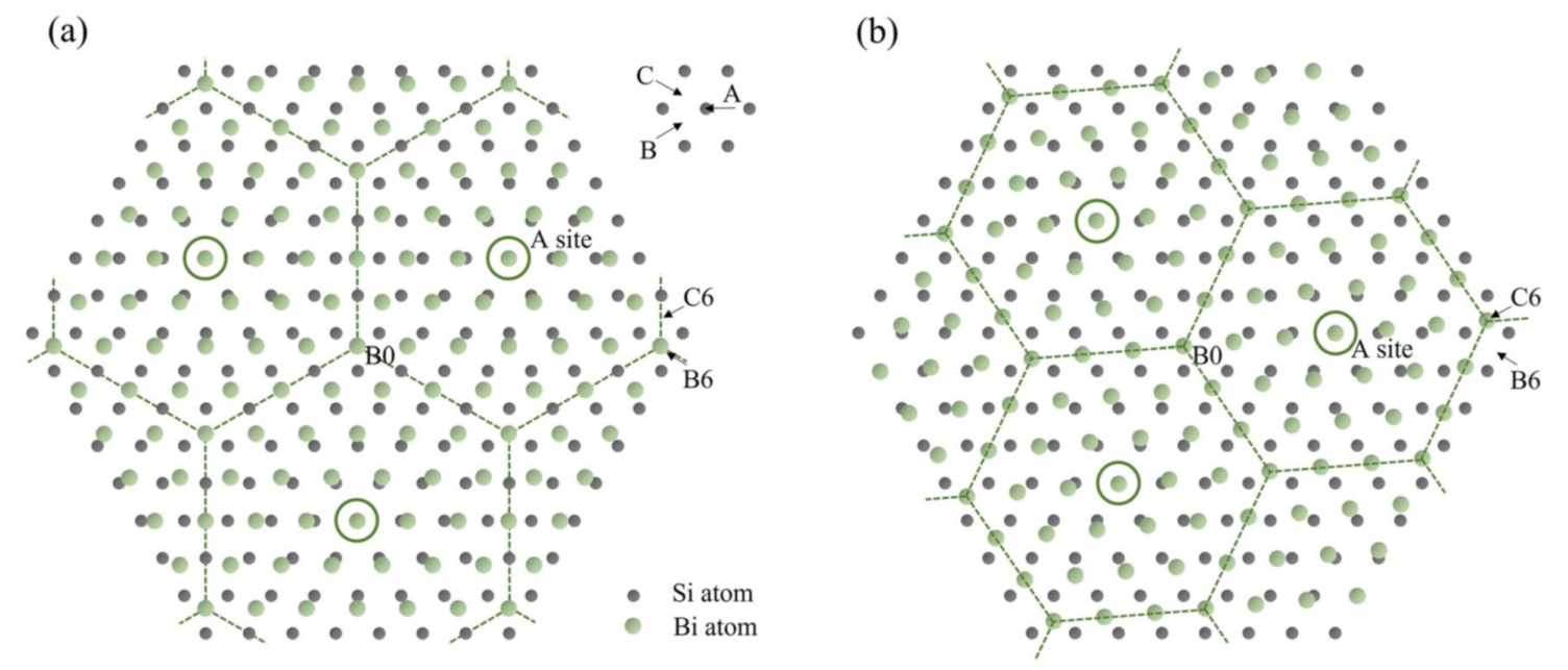
as well as b, the bilayer thickness, determined from XRD for an 80-nm-thick Bi layer, are all within 0.1% as compared with those of bulk Bi, suggesting that the Bi film is nearly fully relaxed. The rapid relaxation despite the huge 18% lattice mismatch is attributed to the quasi-van der Waals bonding at the Bi/Si interface. From the XRD φ-scans of asymmetric Bi (01-14) planes and Si (220) plane, we confirmed the well registration between the lattices of Si and Bi lattice. For the ~10-nm-thick layers, a strain ~2% is observed. From (01-14) φ-scan, we observed an additional rotation phase. We proposed a preferential closed-pack A-B-C site model to explain the observed rotation phases.
|

|
|
Fig. 1. (a) Ω-2θ scan showing the nearly fully relaxed (0003) Bi phase. (b) A (01-14) ϕ-scan showing the dual-peak twinning Bi phases. One of the phases aligns the (220) of Si substrate. EBSD inverse pole figure shown in the inset, green and blue represent the regions of the two twinning phases.
|
|

|
|
Fig. 2. Two Bi atomic arrangements based on preferential site model. (a) Bi hexagonal lattice aligns Si lattice with 6aBi = 7aSi and (b) Arrangement for the rotation phase with tilted Bi hexagonal lattice and 6aBi = 7.024 aSi. The preferential sites in both figures form superlattice indicated by dashed hexagons.
|
|