|
|
 |
| |
發行人:黃建璋所長 編輯委員:曾雪峰教授 主編:林筱文 發行日期:2020.11.30 |
| |
|
 |
~ 2020 第七屆海峽兩岸寬能隙半導體研討會-首次視訊會議 花絮報導 ~
(時間:109年10月22日至23日;地點:臺灣大學博理館201會議室)
花絮整理:李翊綸
原訂今年於台灣舉辦之「第七屆海峽兩岸寬能隙半導體研討會」,因COVID-19疫情關係,兩岸專家學者及產業先進無法齊聚一堂,在台北及花東共同切磋。經兩岸主辦單位討論,所有與會學者以及產業先進於2020年10月22日至23日分別聚集大陸及台灣,以兩地實體會議地點的網路相互連線,採用遠距視訊會議的方式辦理。因此,這是我們首度舉辦「海峽兩岸寬能隙半導體研討會」視訊會議,一共有來自台灣、大陸各個城市40餘位重要專家學者一同在線上共襄盛舉。
本研討會旨在促進兩岸寬能隙半導體研究領域的專家學者及產業界先進進行深入交流,會議主題涵蓋III族氮化物半導體、II-VI族半導體、氧化物半導體等相關材料製備及其應用。本次會議進行方式為台灣、大陸與會者輪流進行專題報告、圓桌論壇以及綜合討論,展開深入的學術研討。
|
 |
 |
|
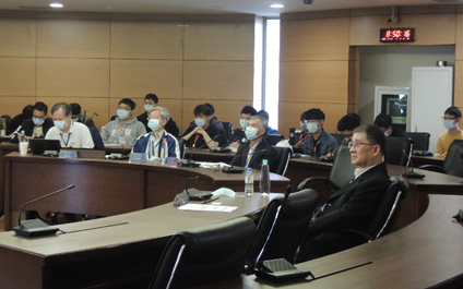
圖一、會議照片 |
圖二、開幕式,會議主席黃建璋教授致詞 |
一場成功的視訊會議仰賴電腦、直播設備以及順暢的網路才得以圓滿,可是我的電腦技能普通,也沒有舉辦視訊會議的經驗,心情緊張程度可想而知。好在會議主席黃建璋教授的學生集結一支「搶救尼安德塔人大兵」,負責架設會議視訊設備以及會場主控導播工作;另一支「外場服務大軍」由本所楊志忠教授助理張珮小姐以及黃建璋教授學生一同協助接待來賓、餐點佈置以及環境整理等事務。
會議的第一天我們跟大陸會場約定早上7:30進行最後的會前測試,同學們早上6:30就抵達會場預備,還準備烤麵包機、吐司跟各類抹醬一起吃早餐。會議閉幕結束後大家邊整理會場邊聊天,笑聲不斷,黃建璋教授也陪我們收拾完畢才離開,充分展現我們是一個team的態度。
|
 |
 |
 |
|
圖三、視訊主控台以及負責同學 |
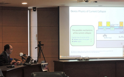
圖四、黃建璋教授進行專題報告 |
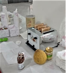
圖五、今天起得早,一起烤土司吧 |
記得茶會的時候有一位教授曾說:「沒想到我們才來兩天,你們要籌備一個月!」在此特別感謝臺大教學發展中心暨數位學習中心出借部份設備,對於網路直播等技術層面也提供我們諸多寶貴建議。感謝臺大光電所所辦同仁以及張珮小姐提供行政流程方面的協助、感謝黃建璋教授的學生利用課餘時間大力相助、感謝電機系系辦網路管理員以及博理館管理中心同仁的幫忙,讓我們在這特別的一年依然能邁出步伐向前衝,舉辦首次「海峽兩岸寬能隙半導體研討會」視訊會議。
|
 |
|
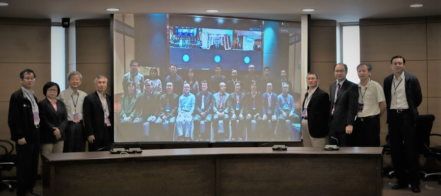
圖六、台灣與會師長與投影幕中的大陸與會專家的團體照 |
|
 |
|
|
|
|
|
|
|
|
|
 |
|
| |
|
|
|
Synthesizer-free 28-GHz MMW Fiber-wireless Link with Orthogonally Polarized Dual-mode VCSEL
Professor Gong-Ru Lin’s Laboratory
Graduate Institute of Photonics and
Optoelectronics, National Taiwan University
臺灣大學光電所 林恭如教授
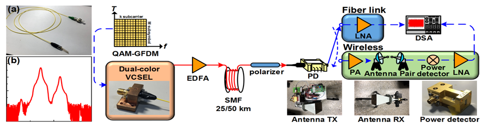
A synthesizer-free 28-GHz is proposed for fifth-generation (5G) millimeter wave over fiber (MMWoF) link by using orthogonally polarized dual-mode vertical-cavity surface-emitting laser (VCSEL) as the frontend transmitter, and the power envelope detection is employed for self-heterodyne down-conversion of the generalized frequency division multiplexing (GFDM) data stream. The demonstrated MMWoF link exhibits superior immunity to the residual frequency and phase noises as well as the inter-carrier interference induced by the free-running dual-mode carrier. After equalizing the dual modes with an extremely weak power as low as -26 dBm at TM-mode polarization, the dual-mode power extinction of only 5.4 dB is achieved for optimizing the remote-node optical heterodyne of 28-GHz MMW carrier with a peak power of -59.8 dBm before antenna propagation with remaining similar relative intensity noise (RIN) as compared to the free-running case. Moreover, the mode partition noise (MPN) is increased less than 2 dBc/Hz after mode-power equalization.
|
|
|
Fig. 1 Schematic diagram of 5G MMWoF link based on 2-l VCSEL transmitter with novel QAM-GFDM.
(a) The
photograph
and (b)
the
optical
spectrum
of
2-l VCSEL without package. |
 |
|
|
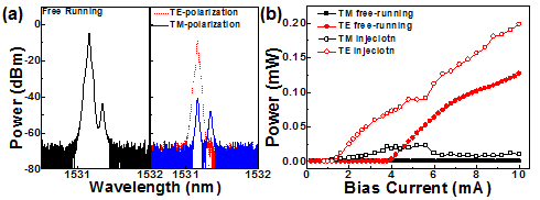
Fig. 2 (a) The free-running polarization characteristic and (b) the P-I curves without and with master controlling of the dual-mode VCSEL. |
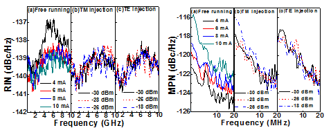
Fig. 3 The RIN and MPN of the dual-mode VCSEL at (a) free-running operation with different bias current and (b) TE- (c) TM-mode injection controlling. |
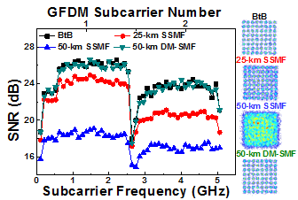
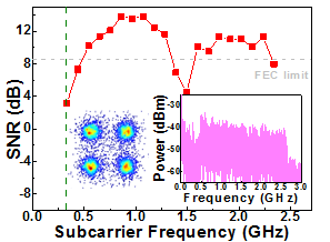
For back-to-back optical downstream wireline transmission, the receiving GFDM data optimizes its BER to 2.2 ´10-4 by adjusting the bias current of the dual-mode VCSEL to 8 mA (3 Ith), and by grouping the GFDM data matrix with total symbols of
N=K´M with
K=2 subcarriers and
M=24 timeslots. After long-reach 50-km DM-SMF, the qualified receiving power sensitivity is -12 dBm, whereas the decoding GFDM data reveals improved receiving sensitivity with extremely low power penalty of only 0.3 dB. After wireless delivering over 2 m in free space, the self-heterodyne down-conversion by power envelope detection guarantees the down-converted QAM-GFDM data stream with an average power of -48.4 dBm after optimizing the impedance matching by selecting appropriate frequency response of the power envelope detector. As a result, the wireless MMW transmission of 8-Gbit/s 4-QAM GFDM data stream is qualified with EVM of 16.9%, SNR of 8.5 dB and BER of 3.8´10-3.
 |
|
|
Fig. 4 The constellation plots and decoded SNR spectra of the modulated 30-Gbit/s 64-QAM GFDM data by the dual-mode VCSEL after BtB, 25-/50-km SMF and 50-km DM-SMF transmissions. |
Fig. 5 The constellation plot, RF and SNR spectrum of the delivered 4-QAM GFMD data after 2-m free-space transmission and self-heterodyne down-conversion. |
Reference:
[1] C.-Y. Lin, Y.-C. Chi, C.-T. Tsai, H.-Y. Wang and G.-R. Lin, “39-GHz millimeter-wave carrier generation in dual-mode colorless laser diode for OFDM-MMWoF
transmission,”
IEEE
J. Sel. Top. Quantum Electron.,vol.
21, no. 6, pp. 609-618, 2015.
[2] C.-T. Tsai, C.-H. Lin, C.-T. Lin, Y.-C. Chi and G.-R. Lin, “60-GHz millimeter-wave over fiber with directly modulated dual-mode laser diode,”
Sci Rep,
vol. 6, no. 27919, pp. 1-12, 2016.
[3] C.-Y. Lin, Y.-C. Chi, C.-T. Tsai, H.-Y. Wang, H.-Y. Chen, M. Xu, G.-K. Chang and G.-R. Lin, “Millimeter-wave carrier embedded dual-color laser diode for 5G MMW of link,”
J. Light. Technol.,
vol. 35, no. 12, pp. 2409-2420, 2017.
[4] C.-Y. Lin, Y.-C. Chi, C.-T. Tsai, H.-Y. Chen and G.-R. Lin, “Two-color laser diode for 54-Gb/s fiber-wired and 16-Gb/s MMW wireless OFDM transmissions,”
Photonics Res., vol. 5, no. 4, pp. 271-279, 2017.
[5] Z.-K. Weng, Y.-C. Chi, H.-Y. Kao, C.-T. Tsai, H.-Y. Wang and G.-R. Lin, “Quasi-color-free LD-based long-reach 28-GHz MMWoF With 512-QAM OFDM,”
J. Light. Technol.,
vol. 36, no. 19, pp. 4282-4297, 2018.
A New Fitting Method for Ambipolar Diffusion Length Extraction in Thin Film Structures Using Photoluminescence Measurement with Scanning Excitation
Professor Ming-Hua Mao’s Laboratory
Graduate Institute of Photonics and
Optoelectronics, National Taiwan University
臺灣大學光電所 毛明華教授
A new simple method is proposed to extract the ambipolar diffusion length for two-dimensional (2D) electronic transport in thin film structures using a scanning photoluminescence microscopy (SPLM) setup. No spatially-resolved photoluminescence detection methods are required. By measuring the excitation-position-dependent PL intensity across the edge of a semiconductor, ambipolar diffusion length can be extracted from the SPLM profile through a simple analytic fitting function. Numerical simulation was first used to verify the fitting method. Then the fitting method was applied to extract the ambipolar diffusion length from the measured SPLM profile of a GaAs thin film structure. Carrier lifetime was obtained in an accompanying time-resolved photoluminescence measurement under the same excitation condition, and thus the ambipolar diffusion coefficient can be determined simultaneously. The new fitting method provides a simple way to evaluate carrier transport properties in 2D electronic transport structures such as thin films or quantum wells. This work has been published in Scientific Reports:
Chu, C. H., Mao, M.-H., Lin, R. Y. & Lin, H. H. A New Fitting Method for Ambipolar Diffusion Length Extraction in Thin Film Structures Using Photoluminescence Measurement with Scanning Excitation.
Scientific Reports
10,
5200, doi:10.1038/s41598-020-62093-w (2020).
|
|
|
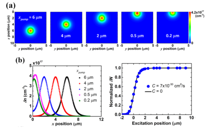
Fig. 1 (a) 2D photocarrier distribution mappings under CW excitation with varied excitation position (x,y) = (xpump,0). (b) Cross-sections of the above mappings at
y = 0 & scanning profile for the normalized total photocarrier number
δN under pulse excitation. The result without Auger recombination is also shown for comparison. |
|
|
| |
|
|
|
|
|
|
| |
|
|
|
論文題目:金屬碘化物於光電電子元件之研究
姓名:李家碩 指導教授:吳志毅教授
| 摘要 |
|
金屬鹵化物為當今熱門研究主題之一,其中最為注目的鈣鈦礦材料具有優越的光電特性,已被廣泛應用於光電、電子元件中,例如電阻式記憶體。由於低製成成本、高可調變性及可媲美或甚至更高的效能,可望取代傳統製成的材料。但材料中含有有毒元素鉛及大氣下結構不穩定性問題,因此本論文將無毒金屬鹵化物材料(碘化鉍)取代鈣鈦礦作為電阻式記憶體阻值切換層。本論文可以分成兩部分,前半部分探討以鉛鈣鈦礦材料為主動層其元件的異常現象:光浸潤效應以及可調變光電流方向現象,並利用調變元件結構抽絲撥繭找出主要因素為哪層或是哪些異質結構影響,並且利用光電子能譜探討載子於介面能階傳輸機制以及材料於持續照光下,材料原子間鍵結變化,並且提出可能機制。而後半部分探討層狀碘化鉍材料做為軟性電阻式記憶體阻值切換層可行性,在探討其與下電極材料間的交互作用中發現,電極基材的化學特性對於碘化鉍的表面形貌、化學鍵結、結晶性以及電阻切換特性有莫大的影響,亦發現碘化鉍缺陷(金屬鉍)的含量對於生成電壓有很大的影響,因此本文提出三種方法改善碘化鉍的表面形貌、化學鍵結及結晶性:透過使用金屬銀當作下電極緩衝層、自組裝分子介面改質以及凡德瓦爾材料作為緩衝層,其中以凡德瓦爾材料作為緩衝層最具廣泛性,其元件可達成無需生成電壓、低操作電壓以及高記憶體視窗,且具高彎折忍受力。本研究不只展現碘化鉍作為可撓式電阻式記憶體切換層的高潛力,其與金屬材料交互作用的探討,亦將有助於其他碘化鉍元件的應用與設計。
|
|
|
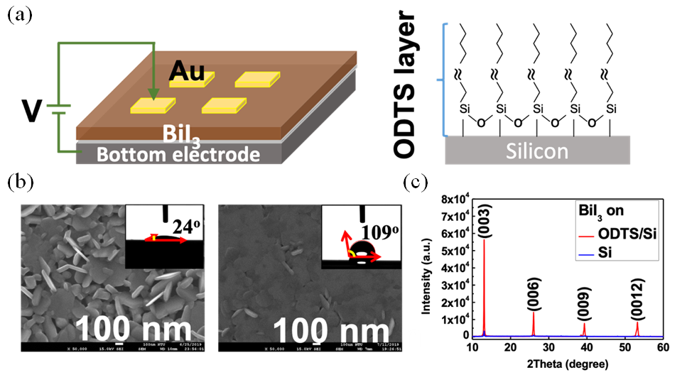
圖一、(a)電阻式記憶體結構圖(左)與自組裝分子ODTS與矽基板鍵結示意圖(右)
(b)碘化鉍在有(右)、無(左)自組裝分子修飾之矽基板之電子掃描顯微鏡圖
(c)為碘化鉍在矽基板之X射線繞射圖 |
|
|
|
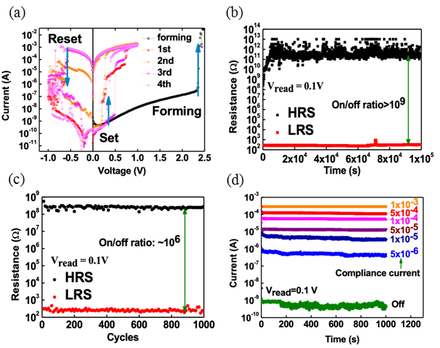
圖二、(a) Si/ODTS/BiI3/Au元件之阻值切換特性圖
(b) Si/ODTS/BiI3/Au元件阻值隨時間變化特性圖
(c) Si/ODTS/BiI3/Au元件對於電壓可容忍性特性圖
(d) Si/ODTS/BiI3/Au元件多階段存取特性圖 |
|
|
|
|
|
|
|
|
| |
|
|
|
—
資料提供:影像顯示科技知識平台 (DTKP, Display Technology
Knowledge Platform) —
—
整理:林晃巖教授、卓真禾 —
百萬像素單光子相機
先進的顯微鏡和量子應用(例如亞單擊雜訊成像和量子光學雷達(LiDAR))都可以受益於單光子和高時間解析度低雜訊的檢測功能。過去具有這種能力的檢測器通常被限制在小於1,000的像素數,甚至是單像素的實現。
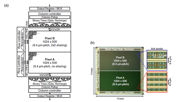
現在,Kazuhiro Morimoto與在瑞士洛桑聯邦理工學院(EPFL)和日本佳能(Canon)公司的同事報導了(Optica 7, 346-354; 2020)一種基於單光子雪崩式二極體陣列的百萬像素光子計數相機(single-photon avalanche diode, SPAD)。其單光子計數解析度與低於100皮秒(ps)的時間解析度是透過一兆像素解析度感測器實現的。相機區塊圖如圖一(a)所示,它包括1024×500像素的兩個獨立部份,其中下半部份陣列基於像素A,上半部份基於像素B。以雙二元樹控制(dual binary tree control)時間閘,其最小長度為3.8奈秒(ns)(可調至9.6奈秒),其變化為120皮秒(半高全寬)。每行在83 ns內被讀出,並分別存儲在晶片底部和頂部像素A和像素B的1024位元和512位元輸出暫存器中。多工器以128位元的字對其進行掃描,然後透過雙並行總線(dual parallel bus)通過128個I/O引腳對晶片外進行傳輸,從而實現24 kfps的幀速率。圖像傳感器的顯微照片如圖一(b)所示。有效區域繪製為圓形,像素A和B的繪製有效直徑分別為2.8微米和3.88微米。
|
|
|
圖一、百萬像素時間閘控SPAD圖像感測器架構。(a)感測器區塊圖;(b)像素陣列的晶片顯微圖和放大圖像素陣列。 |
此相機可以每秒24,000幀的速度運行,並展示了二維和三維成像功能。此相機是EPFL的先進量子架構實驗室在SPAD領域超過15年研究的最高峰。Morimoto告訴《自然光子學》,自2003年以來,當引入互補金屬氧化物半導體(CMOS)SPAD後,他們已經開發出越來越大與更快的相機,其目的是以高保真度和時間解析度捕捉極快的自然現象。
正如Morimoto指出的那樣,SPAD陣列和脈衝雷射可以用於重建毫米級精度的三維場景,即使在遠距離時,這種應用也非常即時,這是LiDAR應用於汽車技術時的核心目標。大型的SPAD相機也可用於顯微鏡檢查,其中超解析圖像的重建具有亞繞射極限解析度。該設置用於捕捉使用其他測距技術難以測量的複雜場景還算足夠靈敏,例如,感測物體通過半透明窗口。
但是這項工作並非沒有挑戰。Morimoto解釋說:「我們的像素尺寸為16微米,我們知道減小的像素尺寸意味著將SPAD縮小到非常小的直徑。」「這是未知領域。此外,鑑於我們用 SPAD的最佳CMOS技術的特徵尺寸為180奈米,每個像素只能提供7個電晶體。因此,我們開始發揮創造力,並分享了所有可能的結構,包括2×2像素中的3個電晶體。這產生了每個像素具有5.75個電晶體的配置。據我們所知,這是有史以來在閘極控制SPAD像素中實現的最少的電晶體。」
高解析度和深度檢測功能也可能對虛擬實境和擴增實境產生影響。Morimoto表示,該技術可以在此類應用中實現更無縫的交互性和更現實的設置。他還解釋說,當在汽車表面使用多個LiDAR設備時,該系統可以實現前所未有的運輸自主性和安全性。在更遙遠的未來,量子通訊,傳感和計算可能會受益於具有數百萬像素解析度的光子計數相機,從而與光學量子位元(qubit)進行交互。
|
參考資料: |
[1] David Pile, “Megapixel single-photon camera,”
Nature Photonics volume
14, 597(2020)
https://www.nature.com/articles/s41566-020-0697-7
DOI: 10.1038/s41566-020-0697-7
[2] Kazuhiro Morimoto, Andrei Ardelean, Ming-Lo Wu, Arin Can Ulku, Ivan Michel Antolovic, Claudio Bruschini, and Edoardo Charbon, “Megapixel time-gated SPAD image sensor for 2D and 3D imaging applications, ” Optica Vol. 7, Issue 4, pp. 346-354 (2020)
https://www.osapublishing.org/optica/abstract.cfm?uri=optica-7-4-346
DOI: 10.1364/OPTICA.386574
|
| |
|
|
|
|
|
|
|
|
|
|
|
|
|
|
|
|
 |
|
 |
|