|
|
 |
| |
發行人:林恭如所長 編輯委員:吳肇欣教授 主編:林筱文 發行日期:2017.10.30 |
| |
|
 |
|
 本所孫啟光教授榮獲教育部「第61屆學術獎—工程及應用科學類科」,特此恭賀!
 本所曾雪峰教授榮獲教育部「106年度友善校園獎—大專校院傑出導師」,特此恭賀!
林清富教授指導本所碩士生同學榮獲「中國電機工程學會106年度青年論文獎第三名」,特此恭賀!得獎名單如下:
|
獲獎同學
|
指導教授 |
論文題目 |
|
郭柏村碩士生 |
林清富教授 |
利用三明治蒸鍍法製備平面異質接面型鈣鈦礦太陽能電池 |
|
|
 |
|
 |
|
| |
|
|
|
|
~ 106學年度光電所所學會會長自我介紹 ~
光電所的師長、所辦同仁以及同學們大家好,我是106學年度所學會會長郭勝文,將會在接下來的一年為大家服務。首先要謝謝上一屆會長蔡瑞祥學長的引薦,在交接會長的過程中幫助我許多,我很榮幸能有機會接下這個職位,也謝謝所辦小姐的幫忙與提醒,希望在這一年能好好經營所學會這個大家庭,延續學長姐們所傳達的精神。
也許新生對於所學會不太熟悉,所以在這邊向大家做個簡單的說明,讓大家對於所學會有個基本的了解。所學會是學生的代表,代替學生爭取應有的權益,且所學會也會負責辦一些活動讓所上的大家有機會互相認識,彼此交流情感,拓展自己的交友圈。
主要的活動有兩個,第一個是上學期的期末餐會,提供美食與表演讓大家快樂地享受,讓各位在研究之旅中,享有一個與所上同儕互動的午後時光,增添在研究所的美好回憶。接著,我們會在下學期舉辦一場球類競賽,競賽的目的不在於輸贏,輸贏只是比賽最後的結果,過程中以球會友、交流球技才是主要的目的。
研究所短短兩年的時間,大家的生活幾乎都在實驗室裡做研究,或是坐在教室看著黑板,體會字裡行間的奧秘,這些確實重要,但人際交流也就漸漸疏遠了,也許生活圈就侷限在實驗室裡了。所學會的目的就是幫助大家藉由活動拉近彼此之間的關係,認識新朋友,透過交流互動後才發現原來我們這麼近,人生猶如白駒過隙般稍縱即逝,若不能在這趟研究之旅中留下美好回憶,豈不是太可惜了嗎?我們所學會非常歡迎你的加入,繼續讓這個溫馨的家庭擴大再擴大,讓大家的研究所生涯不只是研究,而是在回憶裡增添回憶,使得積分起來到無限大。
所學會還有許多不足的地方,希望透過大家的參與讓所學會變得更加完整。我是隸屬於吳志毅老師實驗室的碩班新生,歡迎各位如果有其他想法可以寄信至光電所學會信箱,或是歡迎到我們實驗室聊聊,在此謝謝所辦小姐們的幫助,也謝謝指導教授對我們的支持。最後就是誠摯地再邀請大家,不論是新生或舊生,歡迎你的加入,讓所學會更加完整。
|
|
|
|
|
|
|
|
|
|
| |
|
|
|
Multi-Band Infrared Thermal Emitter with Selectable Polarization
Professor Si-Chen Lee’s laboratory
Graduate Institute of Photonics and
Optoelectronics, National Taiwan University
臺灣大學光電所 李嗣涔教授
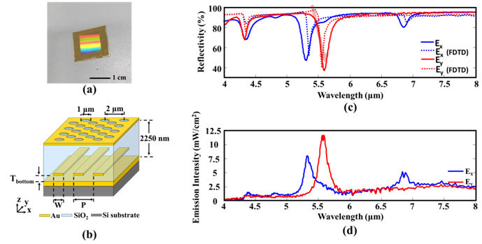
This study demonstrated a multi-band infrared thermal emitter featuring a narrow bandwidth emission and polarization characteristics, which is quite suitable to be applied to the non-dispersive infrared (NDIR) detection system. NDIR system has been widely used in monitoring the hazardous and harmful substances in the human living environment. The target molecules can be detected by measuring the transmission optical energy at specific wavelengths due to their particular molecular bond vibration, which is inversely proportional to the molecular concentration in the NDIR system. Because the biomolecules usually exhibit multiple absorption peaks in the infrared regions, the multi-wavelength infrared light source plays an indispensable role in the NDIR system. The device is constructed by embedding the metallic grating strips within the resonant cavity of a metal/dielectric/metal (MDM) structure, as shown in Fig. 1(a) and 1(b). This arrangement makes it possible to generate waveguide resonances with mutually orthogonal polarization, thereby providing an additional degree of freedom to vary the resonant wavelengths and polarizations in the medium infrared region. The measured reflection spectra and the finite-difference time-domain simulation indicated that the electric fields of the waveguide modes with two orthogonal polarizations are distributed in different regions of the cavity, as shown in Fig. 1(c) and (d). Resonant wavelengths in different polarizations can be adjusted by altering the period, the metallic line width, or the position of the embedded gold strips. The ratio of the full width at half maximum (FWHM) to the peak wavelength was achieved to be smaller than 0.035. This work has been published in AIP
Advances 7, 085122 (2017).
|
|
|
FIG. 1. (a) A photograph of the multi-band infrared thermal emitter with polarized waveguide modes. (b) Schematic diagrams of polarized waveguide thermal emitter. (c) The experimental and FDTD simulated reflection spectra in x- and y-polarizations. (d) The experimental thermal radiation spectra of the device in x- and y-polarizations. |
High-resolution Analysis of Leaky Modes in Surface Plasmon Stripe Waveguides
Professor Hung-chun Chang
Graduate Institute of Photonics and
Optoelectronics, National Taiwan University
臺灣大學光電所 張宏鈞教授
The surface plasmon polariton (SPP) existing at an interface between metal and dielectric material is a basic phenomenon in the area of “plasmonics” and has been a well-known wave mode particularly in the visible and infrared wavelength ranges. With the rapid progress of the plasmonics research in recent years, various SPP waveguides have also been proposed and investigated. Here, we report our recent studies of the stripe plasmonic waveguides with a gold stripe having a silica substrate. Such simple structure was one of the earlier studied SPP waveguides. Weeber
et al.
reported
their experimental measurement results of waveguide mode
characteristics of such structure in 2003 [Phys. Rev. B
68, 115401 (2003)]. Zia
et al. in 2005 [Phys. Rev. B
71, 165431 (2005)] presented finite-difference numerical analysis of the same waveguides, obtained their leaky and bound modes, and concluded that calculated leaky mode characteristics could be consistent with the observed SPP-propagation ones by Weeber
et al. Zia
et al. calculated the real and imaginary parts of the complex effective refractive indices,
neff’s, of the leaky, quasi-transverse-magnetic (quasi-TM) SPP modes for different stripe widths, where
neff is defined as
the modal propagation constant divided by the free-space wavenumber. We have
recently conducted high-resolution finite-element numerical analysis of the same
stripe waveguide using an in-house developed full-vector finite-element
imaginary-distance beam propagation method (FV-FE-ID-BPM) and discovered some
subtle mode-field characteristics in the leaky modes so that the
neff versus the stripe width curves appear to be of non-monotonic variation [H. H. Liu and H. C. Chang, J. Lightwave
Technol.
34,
pp. 2752–2757 (2016)]
|
|
|
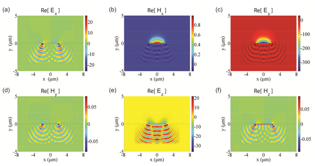
Figure 1 Mode-field profiles of the TM1 mode of the stripe waveguide when the stripe width is 3.7
μm: (a) Re[Ex], (b) Re[Hx], (c) Re[Ey], (d) Re[Hy], (e) Re[Ez], and (f) Re[Hz]. |
Fig. 1 shows the magnitude profiles of the real parts of the six field-component phasors of the lowest TM1 mode for the stripe width of 3.7 μm (the gold stripe thickness is 55 nm). In each panel, the horizontal thin black line shows the boundary of the substrate, and the outline of the boundary of the stripe cross-section appears to be the thicker portion of the thin black line. In the analysis we used 638,347 unknowns for the computational domain of 8 μm x 11.5 μm size, which covers the right or left half of the waveguide cross-section making use of the structure symmetry. Such high spatial resolution and large coverage of the substrate region reveals the details of the leaky fields in the substrate including the interference feature. It is interesting to notice that the two stripe edges provide two sources for the propagating leaky fields. Note that
Hx (Fig. 1(b)) and
Ey (Fig. 1(c)) are the major field components. For further discussions, please refer to [J. Lightwave
Technol.
34,
pp. 2752–2757 (2016)].
|
|
| |
|
|
|
|
|
|
| |
|
|
|
論文題目:提升發光二極體電洞注入效率技術與表面電漿子耦合之薄p-型層發光二極體的特性
姓名:蘇佳瑩 指導教授:楊志忠教授
| 摘要 |
|
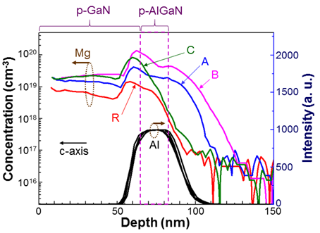
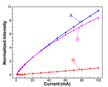
我們提出一個新穎的鎂摻雜技術可提高p-型層的鎂濃度;於p-型氮化鋁鎵或p-型氮化鎵成長之前,於有機金屬氣相沉積系統的腔體中,先吹入鎂金屬源一段時間。提高鎂摻雜濃度而增加電洞濃度於p-型氮化鋁鎵電子阻擋層,尤其是位於發光二極體的電子阻擋層與最上層量子屏障的界面上,可降低電子阻擋層的內部極化電場,進而增加電洞注入效率。於電子阻擋層與最上層量子屏障界面上的鎂濃度可提高約20倍,如圖一內的樣品A與B;發光二極體的發光強度可提升約9.4倍,如圖二的樣品A。並以上述技術成長p-型層厚度僅38奈米的薄p-型層發光二極體,探討表面銀奈米粒子產生表面電漿子耦合效應於不同厚度之p-型層發光二極體的作用。
 |
|
圖一、鎂濃度於樣品中的分布 |
|
 |
|
圖二、發光二極體的發光強度與電流關係圖 |
|
|
|
|
|
|
|
|
| |
|
|
|
—
資料提供:影像顯示科技知識平台 (DTKP, Display Technology
Knowledge Platform) —
—
整理:林晃巖教授、王子聖 —
渦旋式分揀機 (Vortex Sorter)
渦旋光束(optical vortex beam)可用於粒子處理、量子光學、通信及其它應用。在通信中,可以透過具有不同軌道角動量(orbital angular momentum)的空間重疊模態來增加(資料)傳輸量。這些模態可以透過各種龐大的方法,包括:空間光調製器或由計算機數值控制(CNC)路由器或相關銑削方法製作成的厘米級繞射元件去分離或解多工(demultiplexed)。然而,這些元件對於積體化應用(如用於光纖尖端)來說相對較大。
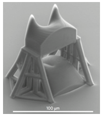
現在,來自以色列的Shlomi Lightman及其同事採用直接雷射印刷技術製造了用於多工(multiplexing)和解多工(demultiplexing)光軌角動量狀態的微米級結構。第一個示範使用了兩個繞射相位元件,而第二個示範則展示了組合所需元件的積體化元件(如圖一所示)。
 |
|
圖一、掃描電子顯微鏡下組合模式分揀機的圖。轉換器和校正元件集成在玻璃基板上,需要相對大的柱體才能進行精確的對準。 |
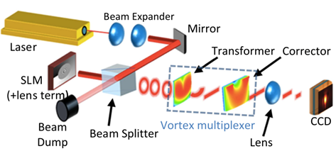
為了研究解多工性能,研究人員產生了不同的渦旋光束。他們對解多工能力進行了測試,但是基於對稱性的考慮,當設備用作多工器時,預期的性能會相同。在CW(是指窄而明確的光譜輻射,亦即連續波)模式中使用具有690-1040 nm可調範圍的Mai Tai鈦藍寶石振盪雷射(Spectra-Physics, USA)。將僅具相位變化之反射式空間光調制器(PLUTO-NIR-011, HOLOEYE, USA) 編程為空間調制光束的相位,接著將光束聚焦到(解)多工器中的附加透鏡項,如圖二所示。一道焦距160 mm、數值孔徑大小為0.01的高斯光束被聚焦到一個56 μm的光點大小(1∕e2),即,約比波長大50倍,因此實驗裝置完全是在近軸的近似之內。
 |
|
圖二、用於測試渦旋多工器的光學設計示意圖 |
研究團隊使用商業3D直接雷射寫入系統印刷了波長在780 nm、而折射率為1.51的材料結構。印刷後,將該結構在顯影劑中漂洗並用異丙醇進行清洗處理。間隔為60 μm之兩個元件(轉換器和校正器)的體積分別為60 × 60 × 32 μm3
和60 × 30 × 51.5 μm3。
在連續波模式中使用由鈦藍寶石雷射照射的僅具相位之反射式空間光調制器產生渦旋光束,產生了從−3ħ到3ħ軌道角動量的光束。在展示中,光束會在每角度動量單位上被空間分離9.4 μm。在此系統中,拓墣電荷必須小於5,但這可以透過調整兩個元件之間的尺寸來增加,作者聲稱系統可以處理10電荷的渦旋光束。研究團隊調整了印刷過程去分析表面粗糙度對設備性能的影響。如預期的那樣,平滑的表面會引起較少的旁瓣和串擾現象。
研究人員對690、790、890和990 nm的波長進行了重複的實驗,並展示了主要局限性為光致抗蝕劑分散的300 nm的頻寬。他們認為,透過設計的優化可以實現波長範圍在300 nm 到2,000 nm之間的操作。 然而,超出該範圍的話,聚合物將變得不透明而應當使用其它材料。
|
參考資料: |
1. David Pile, Vortex Sorter, Nature Photonics 11, 459 (2017)
DOI:10.1038/nphoton.2017.137
http://www.nature.com/nphoton/journal/v11/n8/full/nphoton.2017.137.html
|
|
2. Shlomi Lightman, Gilad Hurvitz, Raz Gvishi, and Ady Arie, Miniature wide-spectrum mode sorter for vortex beams produced by 3D laser printing, Optica 4, 605–610; 201
DOI:10.1364/OPTICA.4.000605
https://doi.org/10.1364/OPTICA.4.000605
|
|
|
|
|
|
|
|
|
|
|
|
|
|
|
|
 |
|
 |
|