|
|
 |
| |
发行人:林恭如所长 编辑委员:吴肇欣教授 主编:林筱文 发行日期:2016.10.31 |
| |
|
|
 |
|
 本所黄建璋教授荣膺「2017 OSA Fellow」,特此恭贺!
 本所林恭如教授指导硕士生同学荣获「中国电机工程学会2016年度青年论文奖」,特此恭贺!得奖名单如下:
第一名:
|
获奖同学 |
指导教授 |
论文题目 |
|
吴采晨硕士生 |
林恭如教授 |
以激光二极管为基础之照明与水下可见光通讯系统 |
第三名:
|
获奖同学 |
指导教授 |
论文题目 |
|
谢政轩硕士生 |
林恭如教授 |
富碳碳化硅波导中非线性克尔与自相位调变全光开关之研究 |
|
|
 |
|
 |
|
| |
|
|
|
|
|
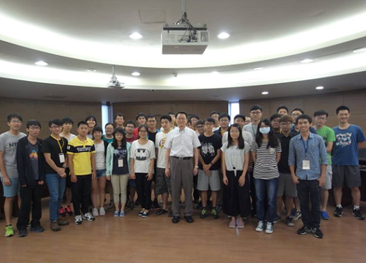
~ 光电所2016年暑期大学生光电营
花絮报导 ~
(时间:2016年8月12日至14日;地点:台湾大学博理馆
)
花絮整理:所学会会长黄郁庭
、活动总召陈惟裕
台大光电所除了专注在研究领域、关心同学的身心健康外,也很注重想来就读的学弟妹们,因此每年暑假都会举办为期三天、从早到晚、包吃包车包上课的精采营队—台大光电营!这个活动是专门为大学部三、四年级的同学举办,旨在向学弟妹们介绍光电领域相关的知识,并介绍所上目前发展的概况,也提供申请方面的信息,对于学弟妹来说是个非常好的机会与体验!
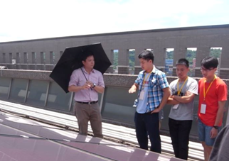
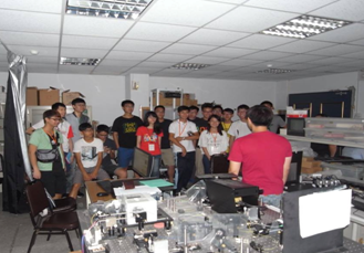
第一天的行程上午为听取教授们专业的演讲介绍,而吴肇欣老师更带同学们去参观博理馆顶楼的太阳能板,亲自顶着严酷的太阳传授同学相关的知识,真是非常令人敬佩!中午吃完美味的便当后,则去参访各个光电实验室,看学长姐们介绍仪器的使用与实验的原理,让各个同学眼睛为之一亮!尤其是林晃岩教授实验室的学长们,更是十分用心地让我们看见全像术的应用,将科技结合生动活泼的影片,促进学习的欲望与研究的动力。
|
 |
 |
|
人称「光电所彭于晏」的吴肇欣老师(左一) |
实验室参访 |
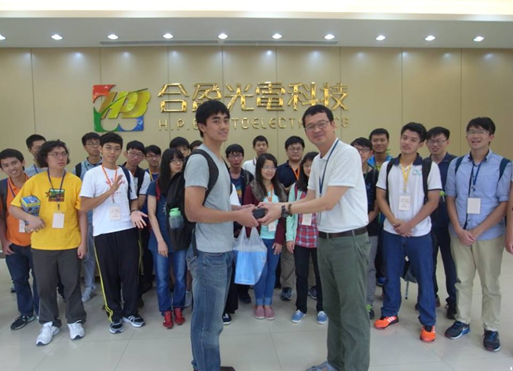
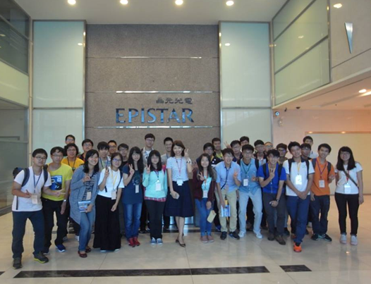
第二天则是前往台中合盈光电及晶元光电的竹南厂进行企业参访。合盈光电让我们参访许多机房,并详细介绍公司发展的历史,也提供茶水点心和餐盒,且让我们体验用手势操控来开车的设备,是间非常棒的公司,欢迎台中来的同学以后可以去就业。下午则是前往晶元光电,现场也备有许多点心,但较遗憾的是无法参观机房只能待在会议室听大姊姊们介绍,但接待人员也都非常亲切!
 |
|
光电营总召—陈惟裕同学(前排左)
|
 |
|
大合照 |
第三天的上午同学们先听了教授精彩的演讲,接着便是大家最期待的行程—手做实验!这次的手做实验课程是实作全息投影(Hologram)以及幻象恐龙(Illusion),我们带着同学们利用透明的投影胶片来制作出简单的小型投影机,配合经过特殊后制的影片,便能直接透过这个投影幕看到立体的影像!而另一个幻象恐龙,则是取材自网络,利用薄薄的一张纸折成的恐龙,却能营造出紧迫盯人的感觉,不管你的头怎么转,他都会对着你看,看的你心里毛毛的!这两项手作实验都得到了同学们的好评,手作期间同学们彼此间的讨论也很热烈,这对于幕后工作人员的我们来说,就是最大的肯定!
用完了精致的午餐之后,同学们带着愉悦的心情迎接最后一门课程,结束之后便是最重要的尾声—颁发证书!所长简单致词后,便在我们所学会同学的协助下,将每位学员的结业证书与光电所精心准备的纪念品亲手颁发给大家,相信每位学员在营队结束之后,一定会将光电营的好宣传给他们的学弟妹们。而随着营队的落幕,我们工作人员也功成身退,相信这几天的美好回忆会永远留存在我们心中!
 |
|
所长与工作人员、所有学员之大合照 |
|
|
|
|
|
|
|
|
|
|
|
|
|
| |
|
|
|
|
High Efficient Planar Heterojunction Perovskite Solar Cells via Sandwich Evaporation Technique
Professor Ching-Fuh Lin’s laboratory
Graduate Institute of Photonics and
Optoelectronics, National Taiwan University
台湾大学光电所 林清富教授
Due to the gradual depletion of fossil fuels, the energy issue has received wide attention in this century. The world is making many efforts to develop alternative energy. Solar energy is an inexhaustible and readily available resources on earth. On the top of that, it is eco-friendly to our environment. For these advantages, the development of solar cells has become an excellent strategy to solve the shortage of energy. Among many types of solar cells, perovskite solar cells suddenly appear on the horizon and the conversion efficiency has been made significant progress from 3% to above 20% in just six years.
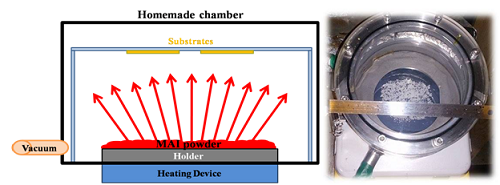
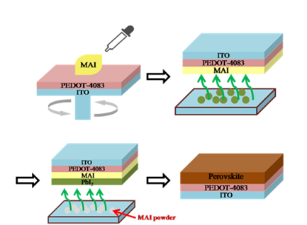
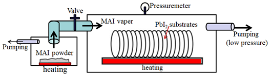
Although high-efficiency perovskite solar cells have been achieved, perovskite formed by solution process, in general, is very susceptible to the atmosphere and moisture. The perovskite grains usually become small and messy by the rapid formation of perovskite. In this research, we developed a new method using a homemade chamber, called Sandwich Evaporation Technique (SET), to form the perovskite layer, as shown in Fig.1. The process can be mostly conducted in the atmosphere and not be affected by the environment easily. The process includes the following steps. First, we raised a sandwich-like structure, MAI/PbI2/MAI, to fabricate the active layer of perovskite to enhance the current density, as shown in Fig. 2. Second, the perovskite solar cells are fabricated with the traditional structure of ITO/PEDOT-4083/Perovskite/PCBM/PEI/Ag, which can successfully achieve the power conversion efficiency of 14.03%.
|
|
|
Fig. 1. The picture of the homemade chamber of Sandwich Evaporation Technique (SET) process. |
|
|
|
Fig. 2. The picture of Sandwich Evaporation Technique (SET) process. |
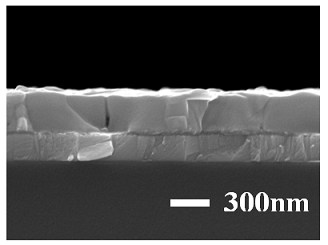
Furthermore, we modify those techniques that can make the better film of the active layer. IPA, CB have been applied on the substrates to slow down the reaction. Here this mechanism is refined for the SET process. Vials with solvent are placed inside the chamber directly. With the refined process, we are able to achieve 14.62% of perovskite solar cells with a higher current density and large crystals of perovskite, as shown in Fig. 3. This brand new method to fabricate the perovskie
under atmosphere environment could potentially
enable the mass production in the future using
the Sandwich Evaporation Technique (SET), as
shown in Fig.4.
|
|
|
Fig. 3. The SEM image of the perovskite. |
|
|
|
Fig. 4. The schematic diagram of the Sandwich Evaporation Technique (SET). |
Improved Internal-Quantum Efficiency of GaN-Based LEDs
Professor Chieh-Hsiung Kuan
Graduate Institute of Photonics and
Optoelectronics, National Taiwan University
台湾大学光电所 管杰雄教授
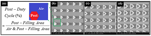
Instead of the limited exposure feature sizes of conventional photolithography, the ELIONIX ELS-7000 E-beam lithography system and the wet-etching technology were conducted to carry out the investigation. All patterned-sapphire substrates (PSSs) were all arranged in squares with the period of 2000nm and with various post-duty cycles (PDCs) of 1, 4 and 8%, which is defined in Fig. 1(a), respectively. Each square had a hexagonal post. SEM images of accomplished PSSs are shown in Fig. 1(b)-(d). The PSSs and a conventional sapphire substrate (CSS) with polished surface were grown using low pressure metal organic chemical vapor deposition (LP-MOCVD). The light-emitting diodes (LEDs) were encapsulated with TO-46 metal can package with a chip size of 17×34 mil2.
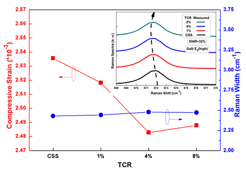
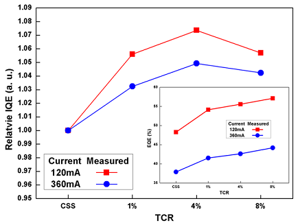
Figure 2 shows the residual compressive strain and the associated Raman width of the GaN-based PSS LEDs. With the increase of PDC, the residual compressive strain of the GaN-based PSS LEDs reduces first and then slightly increases as compared to the sample with the CSS. Fig. 3 shows the relative IQE versus PDC of the GaN-based PSS LEDs biased at injection currents of 120mA and 360mA, respectively. With the increase of PDC in contrast to the CSS, the reduced residual compressive strain leads to the enhanced relative IQE under the same crystalline quality.
|
|
|
Fig. 1. The SEM images of different PSSs and the definition of post-duty cycle |
|
|
|
Fig. 2. The residual compressive strain with the associated Raman width. The inserted figure is the Raman spectra. |
|
|
|
Fig. 3. The relative IQE of the LEDs, calculated from the inserted figure regarding the EQE versus PDC |
|
|
| |
|
|
|
|
|
|
| |
|
|
|
|
论文题目:表面效应对电阻式内存之影响
姓名:柯志坚 指导教授:吴志毅教授、何志浩教授
| 摘要 |
|
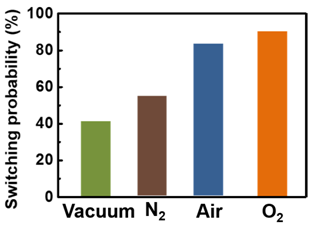
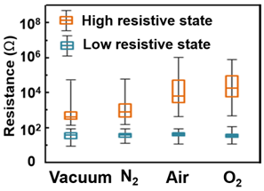
在本论文中,我们展示了表面效应对氧化锌电阻式内存(resistive random access memory)的电阻转换现象有很大的影响。分析了超过400个电阻式内存组件在不同气氛下的电性,我们发现到表面效应(surface effects)对电阻转换的影响。如图一所示,在富氧的环境下,氧化锌电阻式内存有较佳的电阻转换机率。图二显示不同气氛对高阻态(High resistive state)与低阻态(Low resistive state)的影响。分析结果表明氧化锌表面的吸附氧气分子与氧缺陷构建的奈米灯丝两者的交互作用,对电阻式记忆的电阻转换扮演很重要的角色。此外我们也发现到电阻转换机率可以藉由表面粗糙度来调控,表面较粗糙的氧化锌电阻式内存有较佳的电阻转换机率以及在不同气氛环境下电性较为稳定。我们也做了电极相依性的研究,结果显示金属铂的气体吸附活化能较低,于是使用铂作为氧化锌电阻内存的电极有较佳的表现。
 |
 |
|
图一、不同气氛下的氧化锌电阻式内存电阻转换率。富氧环境的转换率较佳。 |
图二、不同气氛对高与低阻态的影响。 |
|
|
|
|
|
|
|
|
| |
|
|
|
|
— 资料提供:影像显示科技知识平台 (DTKP, Display Technology
Knowledge Platform) —
—
整理:林晃岩教授、林暐杰 —
动量多路复用技术
美国著名电影制片厂迪斯尼,可能是你最不会期望对于光的轨道角动量(orbital angular momentum, OAM)有兴趣的组织。不过迪斯尼在加州的研究团队和英国剑桥大学的光子与传感器团队,正连手研究根据OAM多路复用技术为基础的未来3D显示器。
近年来关于扭曲的波前携带OAM的光束之研究一直非常活跃,主要是由于这类光束可形成一组无限数量的正交模态,每个模态可以由扭转量唯一定义。这种特性已经被证明,对于提高基于自由空间和光纤的光通信数据容量,是一种有用而创新的多路复用技术。OAM多路复用技术是很吸引人的,因为它是一种新的自由度,且和现有常见的基于波长、偏振和时间之多路复用技术方案可能兼容。
现在Daping Chu和他的同事正在探讨利用OAM模态,来表现一个物体之不同视角的影像,然后可以利用多路复用技术建造一个多视角3D显示器。目前,研究人员已经展示了基于该方法的三个视角之立体显示器,将三个不同视角的影像编码成OAM光束的数组,则观看者在空间上可接收到分离的三视角之影像显示。
|
 |
|
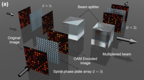
图一、利用光的轨道角动量之多视点3D显示器的示意图。 |
Chu解释说:「将其数目规模放大并不会成为一个问题,至少达成几十个视角影像,换言之将立体影像信息编码为更多模态;然而,在技术上的挑战是如何利用多路复用与解多路复用技术,将多个影像在空间上合成与分开。」
|
 |
|
 |
|
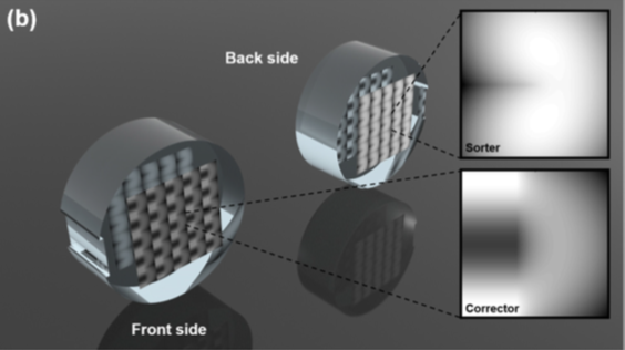
图二、(a) 三个OAM状态之多路复用传输影像的概念图。(b) 设计分拣器和校正器对于OAM光束晶格数组进行分拣,其中分拣器和校正器的高度轮廓分别示于插图。 |
研究团队首先使用一个螺旋相位板来建立所需的OAM模态,然后使用硅基空间光调制器(LCoS)编码的达曼光栅(Dammann grating)来复制光束,以此建立9×9正方形晶格排列之相同OAM的光束。然后三个这样的OAM光束数组各携带不同数量的扭曲波前,被引导到三个影像屏蔽以代表物体的不同视角之影像。这些以不同视角影像加以编码光束,可再用分光束器组合以建立一个多路复用的输出。
然后,该输出经过OAM分拣器进行解多路复用,分离成为不同的OAM光束,OAM分拣器将具有不同方位角相位梯度(即扭转的波前量)的OAM光束转换成一个倾斜平面波,即传播在不同角度的平面波。目前由于分拣器的设计中,每个视角影像之角度间隔(约0.015°)与传统的多视角显示器(其角度间隔通常是0.7°或更大)比较起来是非常小,然而该团队说,应该可以藉由分检器的制造来解决这个问题。
至于该研究领域未来的工作中,Chu说该小组目前正在开发一种方法,不需要藉由像素化,直接将2D影像编码为OAM光束。
|
参考资料: |
1. David Pile, Nature Photonics 10, 570 (2016)
doi:10.1038/nphoton.2016.171 Published online 31 August 2016
2. Li, Xuefeng, et al. "Automultiscopic Displays based on Orbital Angular Momentum of Light." J. Opt. 18 (2016).
doi:10.1088/2040-8978/18/8/085608
|
| |
|
|
|
|
|
|
|
|
|
|
|
|
|
|
|
|
 |
|
 |
|