|
|
 |
| |
发行人:林恭如所长 编辑委员:吴肇欣教授 主编:林筱文 发行日期:2015.08.30 |
| |
|
|
 |
High two-dimensional electron mobility in
a SiGe/strained Si/SiGe quantum well
Professor Chee Wee Liu
Graduate Institute of Photonics and
Optoelectronics, National Taiwan University
台湾大学光电所 刘致为教授
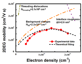
The two-dimensional electron gas (2DEG) mobility has reached 2 × 106 cm2/V s at 0.3 K for 15 nm strained Si well with a 526 nm Si0.86Ge0.14 barrier layer. The SiGe/strained Si/SiGe heterostructure was grown on p-type (001)-oriented Si at 550℃ by hot-walled ultrahigh vacuum chemical vapor deposition. The factors that limit the mobility are the background charges, the threading dislocation density and the roughness at the Si/SiGe heterojunction. Reduction of Ge concentration in the SiGe barrier layer and the relaxed buffer layer that reduces the threading dislocation density and the roughness, effectively enhances the mobility of the 2DEG in the Si channel. The background doping was greatly reduced by high purity gases and the long-time baking of quartz tube.
 |
 |
|
Figure 1. Electron density dependence of the 2DEG mobility for the sample with Si0.86Ge0.14 relaxed buffer layer measured at T = 0.3 K. The maximum value of 2DEG mobility of the Si0.86Ge0.14 sample reaches 2 × 106 cm2/V s at the electron density of 1.4 × 1011 cm-2. |
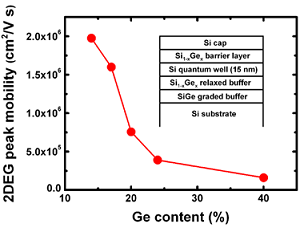
Figure 2. The 2DEG peak mobility as a function of Ge concentration in the relaxed buffer layer. The inset demonstrates the SiGe/Si/SiGe heterostructure schematically. |
Threshold voltage controlled by gate area and gate recess in inverted trapezoidal trigate AlGaN/GaN MOS-HEMTs with PEC and PEALD oxides
Professor
Lung-Han Peng
Graduate Institute of Photonics and
Optoelectronics, National Taiwan University
台湾大学光电所 彭隆瀚教授
An enhancement-mode, AlGaN/GaN
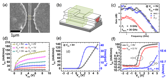
inverted trapezoidal trigate MOS-HEMT wrapped with double-layered oxides, i.e., PEC-grown Ga2O3/(Al,Ga)2O3 and PE-ALD Al2O3, was demonstrated to exhibit positive Vth = 1.2V with current on/off ratio of 108 and sub-threshold swing of 160mV/dec. HRTEM analysis revealed trapezoid-shape channel sidewalls due to crystallographic wet chemical etching by using molten KOH, and a reaction rate-limited process at which the outer surfaces of the nonpolar/semipolar GaN facets are converted into crystalline α-Ga2O3 passivation layers with preferential growth of (003) α-Ga2O3 upon the c-plane of GaN. From DC characteristics analysis of diverse gate recess depths and different gate areas of fabricated devices, we suspected that there is negative polarization in the interface of double-layer gate oxide and barrier to compensate the strong polarization charge induced by AlGaN/GaN heterostructure, and hence, to lead to higher threshold voltage than other HEMTs without gate oxide. These observations can be ascribed to combined effects of (a) interfacial negative space charge of 3.2 μC/cm2 in the gate-recessed device to partially compensate the spontaneous charge, and (b) side-wall passivation to preserve the high mobility channel. It relaxes the constraint of using nanometer scale channel width to achieve positive value of Vth and results in a cut-off frequency of unity current gain/power gain at fT/fmax = 9/36GHz at gate length/width of LG /Lw = 250 /360nm.
|
 |
|
Fig. 1 (a) Top-view SEM micrograph of inverted trapezoidal trigate AlGaN/GaN MOS-HEMT with gate recess, (b) 3D structural diagram of this device, (c) the fT and fMAX plot corresponding to LG=250nm E-mode AlGaN/GaN inverted trapezoidal trigate MOS-HEMT, and DC measurements for (d) IDS-VDS family curves, (e) transfer characteristics and transconductance curve in linear-scale, (f) transfer characteristics of IDS-VG in log-scale and IG-VG gate leakage current measured in a three-terminal configuration. |
Ref: Po-Chun Yeh, Yun-Wei Lin, Yue-Lin Huang, Jui-Hung Hung, Bo-Ren Lin, Lucas Yang, Cheng-Han Wu, Tzu-Kuan Wu, Chao-Hsin Wu, and Lung-Han Peng," Threshold voltage controlled by gate area and gate recess in inverted trapezoidal trigate AlGaN/GaN MOS high-electron-mobility transistors with photoenhanced chemical and plasma-enhanced atomic layer deposition oxides", Applied Physics Express, 8, 084101, 2015.
|
 |
| |
|
|
|
 |
|
| |
|
|
|
|
论文题目:基于宽带晶体光纤组件之功能性光学同调断层扫描术之研究
姓名:何端书 指导教授:黄升龙教授
| 摘要 |
|
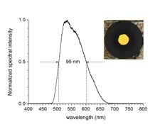
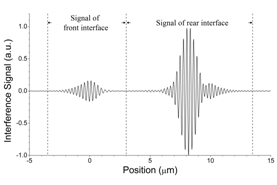
光学同调断层扫描(OCT)除了用来进行结构性的检测外,亦可用来分析材料之光学特性。利用本实验室研发的晶体光纤光源(图一),具有宽带响应之OCT系统可被建立。此OCT系统具有高纵向分辨率(于玻璃中之纵向分辨率达1微米),足以分析微米尺度膜层之特性(图二),而经由OCT获得之数据,除了可准确分析膜层厚度外,亦可量得材料之折射率与消光系数于光源频宽(近95奈米)内之频谱分布。此技术具有高空间分辨率,以及量测结果不易受到样本内未知的结构影响之优点。
 |
 |
|
图一 |
图二 |
|
论文题目:频率选择平面于电磁干扰屏蔽、双频和可调变结构之新颖设计
姓名:黄凡城 指导教授:邱奕鹏教授
| 摘要 |
|
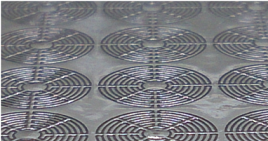
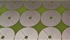
本论文提出新式圆形缩小化结构频率选择平面、非常接近双频频率选择平面以及可调变操作频率的频率选择平面。
新式圆形缩小化结构频率选择平面中提出圆形结构缩小化的设计(如图一),且同时具有其它优点,如对不同极化和入射角度都有稳定结果。非常接近双频频率选择平面(如图二)的主要特点在于两个操作频段可以非常接近,可以更有效的利用频宽。可调变操作频率的频率选择平面则是提出了一个简单可以调整操作频率的方式。
研究中首先会先利用数值仿真软件HFSS(finite element method)进行S参数的分析,观察不同入射角度及极化的频率响应参数,再制作频率选择平面原型以实验量测验证模拟结果。
 |
 |
|
图一、圆形结构缩小化频率选择平面 |
图二、非常接近双频频率选择平面 |
|
|
|
|
|
|
|
|
| |
|
|
|
|
— 资料提供:影像显示科技知识平台 (DTKP, Display Technology
Knowledge Platform) —
—
整理:林晃岩教授、廖玮珅 —
光动能机器人
超微小机器人已经被提出将来可应用于体内药品输送及进行微手术。这样的设备理想上是以无线传输的方式驱动。为了实现这项技术已经有数种方法被探讨,包含使用凡德瓦力(van der Waals)和毛细现象(capillary effects)以及人造肌肉(artificial muscles)。然而要达成微米尺寸之微小化却拥有足够的力量以驱动机器人是一大挑战。
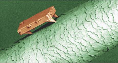
现在Hao Zeng和在意大利和波兰的同事发表了光驱动之显微光行者(walkers) (Adv. Mater. 27, 3883–3887, 2015),此装置尺寸为60 × 30 × 10立方微米(μm3)和四个圆锥形脚长约10微米(如图1),最远可跳1公分远。
 |
|
图1、光能行走者之照片 |
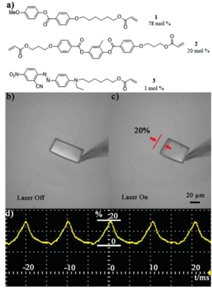
此团队展示一种液晶弹性体(liquid crystalline elastomer, LCE),当使用波长532奈米的激光加热到100 °C时,弹性体可以有20%的收缩(如图 2),这项能力可以被用来驱动经过适当设计的组件脚部。有趣的是,该驱动可以在高达1.8千赫(kHz)的频率下完成。
 |
|
图2、液晶单体成分和LCE致动响应(actuating response)图。(a)实验用分子结构;(b)玻璃上尺寸60 × 30 × 10 µm3 之LCE致动器;(c)藉由聚焦激光加热至100°C时,LCE之收缩情况;(d)相同LCE结构,以100赫兹532奈米激光触发情况。 |
在文章里其中一个作者Diederik Wiersma解释,此系统可被视为是一个微米尺寸机器人(Robot),其优点是可以只藉由吸收环境光而获得能量。对于显微机器人的能量控管一直是一个困难的议题,因为没有任何电池可以做到这么小的尺寸。Wiersma说,「我们以光能解决这个问题。此机器人能走、旋转和跳跃,成为了最小能行走的人造物(artificial creature),比目前已知的地球上动物都还小。」
Wiersma指出他们团队的化学家和物理学家为了这个装置一起工作近五年。工作涉及到了材料科学和光学以及如何使如此微小的装置移动。Wiersma解释:「当你要设计微米等级组件时,物理学上就会变得非常特殊。例如,其黏着力会变得相当的巨大,正确地说,机器人必须利用脚趾的尖端处移动。」
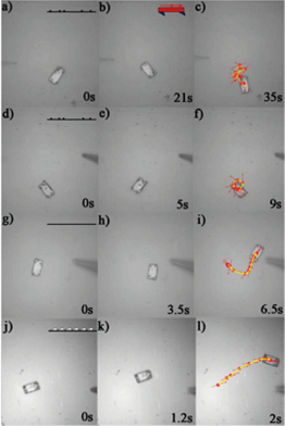
Wiersma指出此概念有助于观察表面的力量及微米尺寸组件的运动,如图3;而另一个有趣的研究面向是,微米机器人不仅可以藉由光能驱动,也可以影响到他们外在环境的光学特性,因此开启了数个研究领域,特别是和不同光学结构的整合。
 |
|
图3、表面运动情形。使用激光(532奈米、50赫兹,每平方毫米10瓦)触发尺寸60微米的显微光行者。(a-c)随机走动在镀上聚酰亚胺(polyimide, PI)的玻璃表面上;(d-f)单脚固定在镀PI玻璃面上旋转;(g-i)自己重新定位到干净的玻璃面上移动;(j-l)沿着垂直光栅槽图案(grating groove pattern)方向移动。 |
|
参考资料: |
1. David Pile,
Micro-optics: Light robots, Nature Photonics 9, 426 (2015).
DOI: 10.1038/nphoton.2015.113, Published online 30 June 2015
http://www.nature.com/nphoton/journal/v9/n7/full/nphoton.2015.113.html
2. Hao Zeng, Piotr Wasylczyk, Camilla Parmeggiani,
Daniele Martella, Matteo Burresi, Diederik Sybolt Wiersma, Light-Fueled Microscopic Walkers, Advanced Materials 27, 3883–3887 (2015).
DOI: 10.1002/adma.201501446
http://onlinelibrary.wiley.com/doi/10.1002/adma.201501446/abstract
|
| |
|
|
|
|
|
|
|
|
|
|
|
|
|
|
|
|
 |
|
 |
|