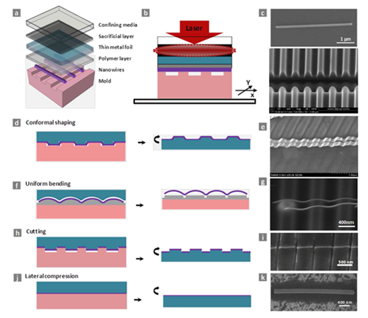
Theoretical Study of Surface Plasmon Coupling between a Radiating Dipole and a Metal Nanoparticle
Professor Y. W. Kiang’s Laboratory
Graduate Institute of Photonics and
Optoelectronics, National Taiwan University
臺灣大學光電所 江衍偉教授
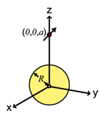
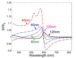
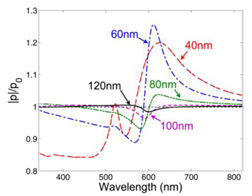
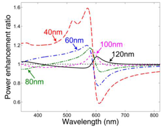
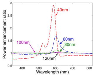
We report the theoretical and numerical study results of surface plasmon (SP)-dipole coupling based on a simple coupling model between a radiating dipole and the SP induced on a nearby Ag nanoparticle (NP). To include the dipole strength variation effect caused by the field distribution built in the coupling system (the feedback effect), the radiating dipole is represented by a saturable two-level system. The spectral and dipole-NP distance dependencies of dipole strength variation and total radiated power enhancement of the coupling system are demonstrated and interpreted. The results show that the dipole-SP coupling can enhance the total radiated power. The enhancement is particularly effective when the feedback effect is included and hence the dipole strength is increased. Figure 1 shows the geometry of the dipole-NP system, including a spherical Ag NP with radius R (=10 nm) centered at the coordinate origin and a radiating dipole located at (0, 0, a), which is represented by an arrow. Figure 2 (3) shows the dipole strength enhancement ratios,  , of the x-oriented (z-oriented) dipole as functions of wavelength when the distance between the dipole and the Ag NP center, a, varies from 40 through 120 nm. Figure 4 (5) shows the total radiated power enhancement ratios as functions of wavelength at several a values for the x-oriented (z-oriented) dipole. The power ratio is defined as the total radiated power of the dipole-NP system over that in the case without the Ag NP.
 |
 |
 |
|
Figure 1 |
Figure 2 |
Figure 3 |
 |
 |
|
Figure 4 |
Figure 5 |
|
Structural properties of InAsPSb grown on GaAs
Professor Hao-Hsiung Lin
Graduate Institute of Photonics and
Optoelectronics, National Taiwan University
臺灣大學光電所 林浩雄教授
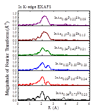
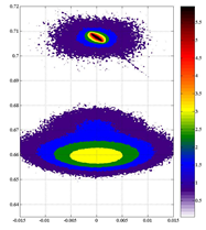
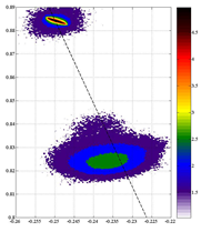
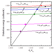
Previous studies have shown that bonds in alloy resemble their original lengths in binaries. Quaternary InAsPSb contains two bonds, InP and InSb, that are with very large mismatch in length. This mismatch leads to strong bond distortion in the quaternary, which could affect the structural, electronic and optical properties. In this work, we investigate the structural properties of InAsPSb grown on GaAs substrate using reciprocal space mapping (RSM) and P K-edge and In K-edge extended X-ray absorption fine structure (EXAFS). Valence force field (VFF) is used to simulate the bond distortion in the quaternary. Fig. 1 shows the Fourier transformed In K-edge EXAFS signals. Two peaks representing InP and InSb bonds are clearly seen when As composition is low and gradually merge into a broad peak with the increasing As composition. Detailed analysis show that the bond lengths are close to their original values in binaries. Fig. 2 shows RSM results of a InAsPSb samples. Although the lattice mismatch between of these alloys and GaAs is ~7% and the layer thicknesses are 1000 times thicker than the critical thicknesses, strong residual strain exists in these layers. We used VFF model to calculate the bond distortion. Fig. 3 shows the distortion energy as a function of az/axy for each sample. As can be seen, the distortion energy is much larger than the strain energy and the residual strain, in term of az/axy ratio, is proportional to the distortion energy. This finding suggests that the randomly oriented bond distortion could hinder the generation of dislocation in the alloy, leading to the observed residual strain.
 |
 |
 |
|
Fig. 1 Fourier transformed In K-edge
EXAFS signal of InAsPSb. |
Fig. 2 (004) and (-1-15) RSM
measurements of InAs0.04P0.73Sb0.23
show a az/axy ratio of 1.017, resulting
from the residual strain in the 1-mm-thick
sample. |
|
|
|
 |
|
Fig. 3 Distortion energy as functions of
az/axy for InAsPSb
alloys. Symbols indicate the az/axy
ratio obtained from RSM measurement for
each samples. |