Combined Experimental and Theoretical Studies on II-VI Ternary CdSeTe and CdZnTe Alloys
Professor Zhe-Chuan Feng
Graduate Institute of Photonics and
Optoelectronics, National Taiwan University
台湾大学光电所 冯哲川教授
The optical, structural, and electrical properties of luminescent II-VI compound semiconductors with bandgap energies ranging from 0 to 4 eV are appealing for ultrasensitive multiplexing/multicolor applications in a variety of emerging areas of biotechnology, nanoscale optoelectronics, and nanophotonics. By varying the composition and controlling the lattice constants in ternary or quaternary alloys, we can achieve greater flexibility of tuning emission and absorption wavelengths for high-efficiency solid-state light emission sources. Earlier, the applications of II-VI materials for photonic devices were hampered primarily by the availability of poor-quality crystals and the difficulty of managing doping. Progress in the modern crystal growth techniques such as metalorganic chemical vapor deposition (MOCVD), molecular beam epitaxy (MBE) etc., has offered higher quality and greater versatility in the preparation of thin films with controlled doping on many convenient substrates.
CdSexTe1-x is the II-VI-VI ternary compound, possesses a zinc-blende structure for x<0.36. The ability to prepare zinc–cadmium (mercury)–based binary [AB, with lended A = Zn, Cd, and Mn (Hg) and B = S, Se, and Te] compounds and thin films of ternary A1−xBxC (e.g., Cd1−xZnxTe, CdTe1−xSex, etc.) or quaternary A1−x−yBxCyD (e.g., Cd1−x−yZnxMnyTe, CdSexSyTe1−x−y , etc. where C and D can be the elements of the binary compound AB) alloys with precise chemical compositions x, y has now opened up many possibilities of using II-VI materials in various technological applications.
 |
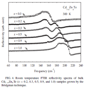 |
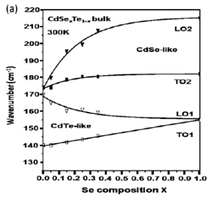
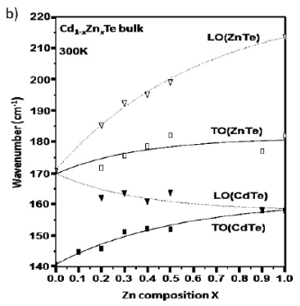
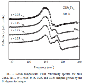
We have measured far-infrared (FIR) reflectance spectra for CdSeTe and CdZnTe alloys, as shown above, and in collaboration with Prof. Devki Talwar, an excellent theorist, also theoretical calculations on their phonon dispersions, as shown below [1]. Further, to II-VI compound semiconductors, we have used a comprehensive Green’s function theory to study the vibrational properties of isotopic defects and to ascertain the microstructure of complex centers involving dopants and intrinsic impurities. [2]
[1] Devki N Talwar, Tzuen-Rong Yang, Zhe Chuan Feng and P. Becla, “Infrared reflectance and transmission spectra in II-VI alloys and superlattices”, Physical Review B 84, 174203 (2011).
[2] Devki N. Talwar, Zhe Chuan Feng and Tzuen-Rong Yang, “Vibrational signatures of isotopic impurities and complexes in II-VI compound semiconductors”, Physical Review B 85, 195203 (2012).
Determination of Surface Plasmon Modes and Guided Modes Supported by Periodic Subwavelength Slits on Metals Using a Finite-Difference Frequency-Domain Method Based Eigenvalue Algorithm
Professor Hung-chun Chang
Graduate Institute of Photonics and
Optoelectronics, National Taiwan University
台湾大学光电所 张宏钧教授
An eigenvalue solution algorithm is formulated based on the finite-difference frequency-domain (FDFD) method for determining guided modes, including the surface plasmon modes, supported by periodic metallic structures. The Yee-mesh grids which have been popularly adopted in the finite-difference time-domain (FDTD) method are used in the FDFD method and standard eigenvalue matrix equations are obtained for easily searching for the guided eigenmodes. Both two-dimensional (2-D) and three-dimensional (3-D) structures are considered and the periodicity is along the propagation direction. The metals are assumed to be perfect ones or real ones without loss. For 2-D structures, an array of grooves drilled in a perfect conductor and a real-metal structure with a periodic arrangement of subwavelength slits in air are analyzed and the dispersion diagrams and mode-field profiles are obtained. For the latter structure, surface plasmon modes and dielectric slab modes are identified to be in agreement with published results based on a different numerical scheme. This subwavelength-slit structure is then extended to a 3-D one having an additional depth and it is demonstrated that the formulated algorithm can solve the same two kinds of modes for the more complicated 3-D problem. The modes guided along drilled periodic rectangle holes on a perfect conductor surface are also calculated. (IEEE/OSA Journal of Lightwave Technology, vol. 30, no. 1, pp. 76–83, 1 January 2012.)
 |
 |
|
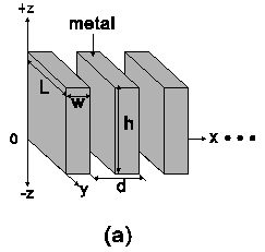
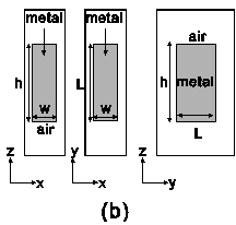
Fig. 1. (a) Schematic of the 3-D
structure generalized from the 2-D
periodic arrangement of subwavelength
slits. (b) Schematic of the three sides
of one metallic block in the x-z,
x-y, and y-z planes. |
 |
|
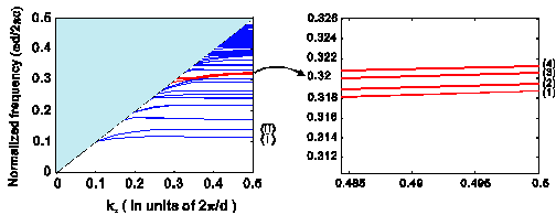
Fig. 2. Dispersion diagram of the guided
modes on the structure of Fig. 1. The
red solid lines represent surface
plasmon modes and the blue solid lines
represent a series of effective
dielectric slab modes. The right panel
is the expanded view for more clear
visualization of the surface plasmon
modes. |
 |
 |
 |
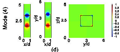 |
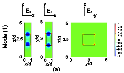
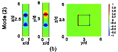
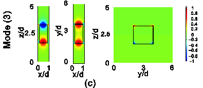
| Fig. 3. Ex field profiles at kx
=
p/d on the three sides of
one metallic block, as plotted in Fig.
1(b), i.e., in the x-z, x-y,
and y-z planes, for each of the
four suface plasmon modes mode in Fig.
2. (a) Mode (1). (b) Mode (2). (c) Mode
(3). (d) Mode (4). |
Regularly Patterned InGaN/GaN Quantum-well Nanorod Light-emitting Diode Arrays
Professor
C. C. (Chih-Chung)
Yang's group
Graduate Institute of Photonics and
Optoelectronics, National Taiwan University
台湾大学光电所 杨志忠教授
With the nano-imprint lithography and the pulsed growth mode of metalorganic chemical vapor deposition, a regularly-patterned, c-axis nitride nanorod (NR) array of quite uniform geometry with simultaneous depositions of top-face, c-plane disc-like and sidewall, m-plane core-shell InGaN/GaN quantum well (QW) structures is formed. The differences of geometry and composition between these two groups of QW are studied with scanning electron microscopy, cathodoluminescence, and transmission electron microscopy (TEM). In particular, the strain state analysis results in TEM observations provide us with the information about the QW width and composition. It is found that the QW widths are narrower and the indium contents are higher in the sidewall m-plane QWs, when compared with the top-face c-plane QWs. Also, in the sidewall m-plane QWs, the QW width (indium content) decreases (increases) with the height on the sidewall. The observed results can be interpreted with the migration behaviors of the constituent atoms along the NR sidewall from the bottom.
 |
 |
|
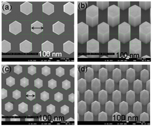
Fig. 1 Plan-view (a) and 30o-tilted (b) SEM images of the GaN NR array; Plan-view (c) and 30o-tilted (d) SEM images of the QW NR array. |
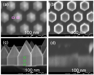
Fig. 2 Plan-view SEM (a) and the co-located panchromatic CL (b) images of the QW NR array; Cross-sectional SEM (c) and the co-located panchromatic CL (d) images of the QW NR array. The rectangles in (a) and (c) indicate the locations of local CL spectrum measurements. |
 |
 |
|
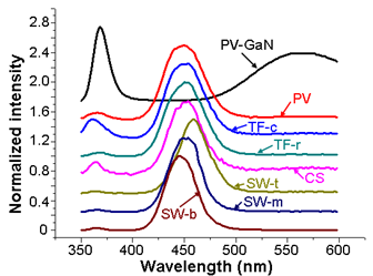
Fig. 3 CL spectra of the QW NR array measured at different locations and different view directions, including that from the large-scale plan-view (PV) measurement, that at the center on the top face of an NR (TF-c) and that at the rim on the top face of the NR (TF-r), that from the large-scale cross-sectional view (CS) measurement, that at a point near the top of the sidewall (SW-t), near the middle height of the sidewall of the NR (SW-m), and near the bottom of the sidewall of the NR (SW-b). The plan-view CL spectrum of the bare GaN NR array is also plotted as curve PV-GaN. |
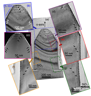
Fig. 4 (a) Cross-sectional TEM image of a QW NR. The portions of the top, the slant (1-101) facet on the right, the top sidewall on the right, the middle-height sidewall on the left, and the bottom sidewall on the right of the NR are magnified to show parts (b) and (d)-(g), respectively. The HAADF image of the NR top portion is shown in part (c). |

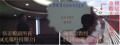
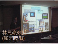
 光电所的各位师长、所办同仁以及同学大家好,很高兴能够担任2012学年度的光电所所学会会长,能为各位服务是我的荣幸。我是陈奕均,名字恰与所上的陈奕君教授差一个字,不过陈奕君教授是取得普林斯顿大学学位的PHD,而我只是个普林含量太高的食物不能吃太多的PHD候选人,目前正向博二的路迈进,目前在林晃岩教授的显示光学实验室下进行研究,研究室位于电机二馆的351A,欢迎各位同学不论是学业上有问题或者对光电所有任何的不熟悉都可以来找我聊聊。