第五十一期 2010年2,3月刊


發行人:黃升龍所長  編輯委員:蔡睿哲教授  主編:林筱文  發行日期:2010.02.15


本所3月份演講公告:

日期

講者簡介 講題 地點 時間

光電論壇

3/9 (Tue)

林清隆教授

Nanyang Professor

Director, Photonics Research Center, School of EEE, Nanyang Tech. University, Singapore

From G. Marconi to Charles K. Kao---100 Years of Nobel Prize (Physics, 1909-2009) and A Century of Modern Marvels of EECS

博理館

101演講廳

16:30~18:30

3/12 (Fri)

Stephen E. Saddow

Professor of Electrical Engineering, University of South Florida

Silicon Carbide: A Robust Semiconductor Material for Harsh Environment MEMS and Biomedical Applications

博理館

101演講廳

14:30~16:30


~ 2009 第一屆微結構攝影競賽得獎作品發表  系列報導 ~ 【六之六】

評選時間:98年8月17日;評選地點:臺灣大學博理館B1博理藝廊)

《創意獎》

【作品名稱】大霹靂
【參賽作者】趙嬿鈞   陳政營   林怡瑞   戴育安
 

【作品說明】


藝術性:

強而有力且令人驚艷的散射狀,讓人聯想起宇宙的發展,是否始於這神奇微小的結構中呢?


實物說明:

此結構為ZnO奈米線球,可以看出ZnO放射狀的結構。此奈米線成長的方向為壓電性最強的c軸方向。 


第二屆國際白光發光二極體及固態照明研討會

【The Second International Conference on White LEDs and Solid State Lighting (White LEDs 2009) 】

(時間:98年12月13-16日;地點:台北國際會議中心

花絮整理:陳雯萍

由本所楊志忠教授舉辦的「第二屆國際白光發光二極體及固態照明研討會」(The Second International Conference on White LEDs and Solid State Lighting 【White LEDs 2009】)已於98年12月13至16日假台北國際會議中心舉行。本研討會為期兩天半,發表文章共計156篇,包含3篇Keynote speech、20篇Invited talk、7篇Industrial forum、41篇報告論文,以及85篇壁報論文。吸引來自奧地利、中國大陸、德國、香港、印度、以色列、日本、韓國、立陶宛、馬來西亞、荷蘭、俄國、台灣、英國、美國等15個國家地區,共計330位相關領域人士參加。研討會包括八大主題,分別為:Semiconductor epitaxial growth and characterization for LED fabrication、Organic/polymer and phosphor material preparation for OLED/LED fabrication、Semiconductor LED design and fabrication、Organic/polymer light-emitting device design and fabrication、Nanotechnology for enhancing emission efficiency、Packaging and system、Various applications、Other LED topics。

此次會議安排相當豐富多元,第一天(12/14)上午為三場Keynote Speeches,邀請美國Rensselaer Polytechic Institute之Fred Schubert教授、University of California at Santa Barbara 之James Speck教授,以及日本Sophia University之Katsumi Kishino教授擔任主講學人;下午則分兩個sessions,分別討論Epitaxial Growth (I)以及Packaging,隨後為85篇壁報論文展示。當晚安排Conference reception。第二天(12/15)上午共有四個sessions,分別為OLED and Phosphor (I)、LED Device (I)、OLED and Phosphor (II)、LED Device (II);下午除了Applications (I)、Applications (II)兩個sessions之外,安排工業論壇(Industrial Forum),邀請七位業界專家發表演說並和與會者進行Panel Discussion。隨後為Conference Banquet。第三天(12/16)上午安排四個sessions,接續主題Epitaxial Growth和LED Device。因本研討會有不少外籍人士參與,特別於第三天下午安排故宮參訪,提供與會者更多面對面交流機會,同時也兼顧文化傳播。

本次研討會於12月中旬舉辦,台北氣候涼爽舒適,且避開其他國際研討會之檔期,外國人士參與踴躍。而場地於台北國際會議中心,硬體設備完善,周圍環境亦佳,對我國國際形象之提昇助益頗大。會議的reception 及 banquet分別邀請蘭陽舞蹈團及漢唐樂府表演特色舞蹈、台灣藝術大學同學演奏國樂,現場佳評如潮。此外,本研討會兼顧理論與實務,特別安排Industrial Forum,邀請來自馬來西亞、美國、台灣、中國大陸、德國、日本、韓國等地之業界專家發表文章及參與討論,現場和與會者互動密切,問答精采,實為國內產學研界難得之技術交流機會。

由於我國不僅是全球LED產量最大國家,相關學術與應用研究水準在全世界也是名列前茅。本研討會在台北舉行第二屆,意義極為重大,共有330人參加,包括本地學術界、業界及研究單位,更有來自世界各國相關領域專家學者參與,誠為我國光電界之一大盛事,對我國相關學術、研發及產業界之發展與能見度提昇將有重大影響。

簽到處 Keynote speech
分組會議 壁報論文展示
Panel Discussion (Industrial Forum) Conference banquet
Conference banquet Invited speakers與漢唐樂府演出者合影


~ 第六屆亞洲區超快現象會議 ~

【Asian Conference on Ultrafast Phenomena】

(時間:99年1月10-13日;地點: 臺灣大學博理館)

花絮整理:焦家洵

本所孫啟光教授在新年的開始,於1月10日至1月13日辦理第六屆亞洲區超快現象會議,總計共有來自10個國家,超過150名的專家學者註冊前來參加會議,同時現場開放光電所、電機系、物理系、化學系等系所的師生免費進場聽講。我們深信舉辦這次國際會議,透過各國間學者的交流與互動,定能達到推廣超快現象研究,整合國內超快現象研究計畫,並促進國內外研究合作等全方位之目的,顯著提升國內高等教育之目標。

亞洲區超快現象會議(Asian Conference on Ultrafast Phenomena)每二年舉辦一次,於1999年首次在韓國舉辦,十年間先後於日本、中國大陸、香港、新加坡等地舉行。本次會議由本所孫啟光教授擔任大會主席,除上述各國外,更有美國、俄國、加拿大、印度等國之學者共襄盛舉。會議研討題目涵括光學、物理、化學、生物等各領域中之超快現象研究,除了讓各國學者有機會分享彼此的最新研究成果外,也是讓國際了解我國研究水準,促成國際合作的重要平台。

本次會議從1月10日開始,為期四天,至1月13日結束。大會在孫啓光教授主持下正式開幕,總計共有35名國際知名學者受邀前來發表專題演講,並收到90篇各國學者投稿之研究論文。孫教授於致詞時表示,亞洲國家數十年來的進步不但有目共睹,更漸漸成為世界重要科技研發之主力。飛秒技術是目前最先進的科研項目之一,飛秒技術不但與超快現象研究息息相關,更影響著臨床醫學、環境能源、高速通訊、奈米纖維、以至於國家安全等各領域之研究。亞洲各國若能加深在超快現象研究領域之交流與合作,必能在國際學術領域尚引領潮流,邁向新的里程碑。

為期四天的會議除了有各國學者受邀發表專題演講外,同時也規劃投稿學者進行現場演講及海報簡介,讓所有與會人士能在現場針對特定題目進行討論。除此之外,在Coherent/SuperbIN公司的贊助下,本次大會也特別舉辦最佳論文競賽,讓投稿的碩博士生與博士後研究員進行演講競賽,角逐大會最佳論文的獎項。本校物理系的廖建盛同學也在眾多的參賽者中脫穎而出,成為五位受獎人之一。

在學術研討以外,本次辦理之國際會議,也希望能增加臺灣大學的國際能見度,提升臺大學術國際化的程度。會議中孫教授亦向各國學者介紹臺大之歷史傳承,臺大在國內的學術地位,及目前進行中的國際合作研究項目。會議期間亦有俄國學者具體提出合作計畫,希望有效地促進兩國間的學術合作。除此之外,孫教授也安排與會來賓參觀故宮博物院外,並向與會學者介紹中正紀念堂、圓山飯店、台北101等北市知名地標,希望能向各國與會來賓介紹中華文物之傳承,並讓與會者體驗台北市多元的面貌。

這次的亞洲區超快現象會議圓滿結束,不但達到原先預定的目標,在整合國內超快現象研究計畫、促進國內外研究合作外,更讓所有工作人員得到寶貴的經驗,在未來更多由本所主辦的國際會議中,能有更完美的表現。在未來的會議中,本所會持續協助本校師生及國內學術界擴大參與各項國際會議,以達到刺激國內外研究合作之目的,以提升國內高等教育為目標前進。


Modal Characteristics of Antiresonant Reflecting Pipe Waveguides for Terahertz Waveguiding

Professor Hung-chun Chang

Graduate Institute of Photonics and Optoelectronics, National Taiwan University

臺灣大學光電所 張宏鈞教授

The pipe waveguide, which is a thin pipe consisting of a large air core and a thin dielectric layer with uniform but low index, is promising for THz waveguiding owing to its low-loss feature and simple structure. In this research, modal characteristics of the leaky core modes of the pipe waveguide are investigated in the THz range. Utilizing the finite-difference frequency-domain (FDFD) mode solver, modal indices and attenuation constants of the core modes which are frequency dependent are calculated for different core diameters, cladding thicknesses, and cladding refractive indices. It is found that at certain frequencies no core modes can exist. Comparing these frequencies with the resonant frequencies of the cladding reveals that the guiding mechanism of the core modes is that of the antiresonant reflecting guiding. Calculated results also suggest that, to have a low-loss and high-bandwidth pipe waveguide, large core diameter, thin cladding thickness, and low refractive index are desired. The effect of material absorption is also examined, which shows that the attenuation constant magnitude will be increased and the increment is more significant at higher frequencies. Moreover, modal patterns are shown for the fundamental mode and the higher order modes, including modal intensity distributions and electric field vector distributions. It is observed that modal patterns of the core modes of the pipe waveguide resemble those of the guided modes of the step-index fiber. From the spectrum of the attenuation constant, it shows that the fundamental mode (HE11-like) has the smallest attenuation constant and is the dominant mode for the pipe waveguide investigated. (Optics Express, vol. 18, no. 1, pp. 309–322, 5 January 2010.)

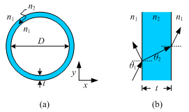
Fig. 1. (a) Cross-section of the pipe waveguide, where n1 = 1 (air). (b) The cladding can be viewed as a Fabry-Perot etalon.

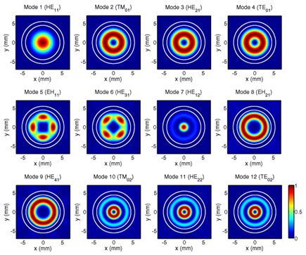
Fig. 2. Modal intensity distributions of the first twelve lowest modes of the pipe waveguide at 380GHz. The parameters of the pipe waveguide are: core diameter D = 9 mm, cladding thickness t = 1 mm, and cladding refractive index n2 = 1.4.

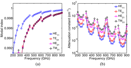
Fig. 3. (a) Modal indices and (b) attenuation constants of the fundamental mode and the first set of higher order modes of the pipe waveguide.


Fabrication of Sphere-like Au Nanoparticles with Laser Irradiation for Localized Surface Plasmon Resonance Applications

Professor C. C. Yang’s Laboratory

Graduate Institute of Photonics and Optoelectronics, National Taiwan University

臺灣大學光電所 楊志忠教授

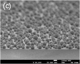
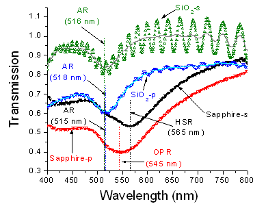
We have demonstrated a simple method for fabricating substrate adhesive Au nanoparticles (NPs) of no aggregation based on a process of laser ablation and annealing. The size, shape, surface density, and coverage of Au NPs on a substrate can be controlled by laser energy density, substrate material and surface condition, deposited Au film thickness, and the liquid covering the Au film during laser irradiation. With optical transmission measurements, the in-plane and out-of-plane localized surface plasmon resonance (LSPR) features can be clearly identified due to the similar shapes and vertical alignments of NPs on substrate. The spectral features of substrate-affected LSPR modes rely on the size, Au/substrate contact area, substrate material, and surrounding gas or liquid. Numerical simulations based on the finite-element method show highly consistent results in the LSPR-induced extinction spectral features. Fig. 1 and 2 show the plan- and tilted-view SEM images of Au NPs on a sapphire substrate. Fig. 3 shows the transmission spectra of Au NPs on sapphire and SiO2 demonstrating the LSPR features. For details, please read the publication: C. Y. Chen et al., Optics Express 17, 14186 (2009).
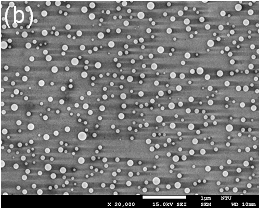
Fig. 1. Plan-view SEM image of Au NPs. Fig. 2. Tilted-view SEM image of Au NPs.

Fig. 3. Transmission spectra of Au NPs on sapphire and SiO2 substrates.


論文題目:以有機金屬氣相沉積法從事氮化鎵奈米柱生長和接合再生長以及其特性研究

姓名:唐宗毅   指導教授:楊志忠教授


摘要

本篇論文主要使用氮化鎵奈米柱接合再生長的方式來減少線差排(threading dislocation)密度。進行方式為:在傳統的氮化鎵基板上,用奈米壓印的方式於表面上製作出週期性孔洞的二氧化矽,再使用脈衝成長模態 (pulsed growth mode)於有機金屬氣相沉積的環境下成長高品質之氮化鎵奈米柱,再將成長模態轉換至二維成長模態進行接合再生長。圖一為接合再生長之氮化鎵基板之掃描式電子顯微鏡(scanning electron microscopy)橫截面影像,並且在原子力顯微鏡(atomic force microscopy)、穿透式電子顯微鏡(transmission electron microscopy)、深度解析X光繞射(depth-dependent X-ray diffraction)、變溫光激發螢光(temperature-dependent photoluminescence)等量測中,都顯示出此一基板之各項性質都比傳統基板更為優越。圖二為電激發螢光(electroluminescence)量測結果,於此基板上成長之藍光發光二極體比成長於傳統基板之發光二極體增加約百分之八十的發光強度。

圖一

圖二


— 資料提供:影像顯示科技知識平台 (DTKP, Display Technology Knowledge Platform) —

— 整理:林晃巖教授、陳冠宇 —

軟性半穿透微型發光二極體顯示技術

美國伊利諾大學香檳分校材料科學教授John Rogers 於2009年八月份Science 期刊發表一項新的發光二極體印刷製程,能夠讓縮小後的LED(light-emitting diode,無機發光二極體)排列出顯示器的畫素單元,此技術讓這些微小發光源更容易且大面積地鑲嵌製作於玻璃、塑膠或橡膠基板等材料上,因此可能會衍生出許多經濟且環保的應用,包含電腦螢幕及可彎曲式顯示器(如圖一),而跳脫過去只能用OLED(organic light-emitting diode,有機發光二極體)來打造類似螢幕的局面。該項研究由伊利諾大學(University of Illinois)材料科學暨工程學系教授John Rogers與西北大學(Northwestern University)、新加坡高性能運算研究所(Institute of High Performance Computing)及北京清華大學的科學家們完成。


常見的LED是由無機材料製成,底層是提供電子的n-type半導體,頂層的p-type半導體層則提供電洞,在適當的外加電壓下,電子與電洞會復合而放出光子。藍光及綠光LED分別是由氮化鎵(GaN)及氮化銦鎵(InGaN)所構成,紅光LED則是由磷化鋁銦鎵(AlInGaP)所構成。無機LED具有高亮度、穩定、壽命長等優點,但製作卻很費工,通常是在基板上生長一層層的半導體薄層,切割成數千晶片,再將晶片鑲嵌在各應用產品中,以目前製程製作出來晶片尺寸皆超過200μm,對許多顯示器來說太大了。 相反的,OLED是在氧化銦錫導電層及金屬層之間夾著數層有機材料所形成的三明治結構,施加電壓時,電子和電洞來自元件兩側,並在有機層復合而產生光子,近年來這項技術已被用來製造顯示器面板。 


要以微型化無機LED製作出顯示器是項艱難的挑戰,但伊利諾大學香檳分校的John Rogers等人辦到了。他們首先在砷化鎵基板上製作紅光LED結構,並沉積一層砷化鋁,然後利用曝光顯影技術選擇性移除砷化鋁,在基板上蝕刻出許多排列整齊、大小約50μm的方塊,再以氫氟酸去除砷化鋁層,在砷化鎵基板上形成LED陣列。接著研究人員由砷化鎵基板取下LED陣列,並置於已預製金屬電極的玻璃、塑膠或橡膠基板,再以曝光顯影技術加上第二組電極,就大功告成了,如圖二。 


Rogers指出,「我們的目標是將無機LED的一些優點與有機LED的高適應性、易生產與易處理的特質相結合,藉著製造出一大排的超薄、超小無機LED,並透過薄膜製程將它們互相串連在一起,我們可以創造出一般的照明系統與高解析度的顯示系統,這是採用傳統製程生產、處理與組裝的無機LED所無法辦到的」。 可彎曲LED網特別適合用在醫療領域,Rogers表示:「將一個可延展的、由小顆LED組成的網子繞在人體上,可提供生物醫學與生物科學有趣的研究機會,這包含了健康監測、診斷、成像等方面的應用」。


該團隊的目標是利用微型LED製作顯示器所需要的畫素陣列,而不只是當背光源使用。雖然目前這項技術只製作出紅光顯示器,但Rogers計畫製作出微型藍光及綠光LED,以達成全彩顯示。其他有潛力的應用,例如:能夠依據裝潢空間造型設計的LED白光面型照明光源;以及和車身型態結合得更美觀的LED方向燈、LED煞車燈等,如圖三。該團隊也致力於發展可撓式紅外光或UV發光裝置,期望能應用於生物醫學上。


圖一、印在一層薄塑膠板上、繞著手指的微型LED顯示器。

圖二、微型化LED製程步驟。

圖三、 可延展的微型LED,印製出來的微型LED相連成一張網,並附著在一個橡膠底層上。


中文新聞來源:

http://taiwan.cnet.com/crave/0,2000088746,20140361,00.htm

原始期刊:

“Printed Assemblies of Inorganic Light-Emitting Diodes for Deformable and Semitransparent Displays”, Sang-Il Park, Yujie Xiong, Rak-Hwan Kim, Paulius Elvikis, Matthew Meitl, Dae-Hyeong Kim, Jian Wu, Jongseung Yoon, Chang-Jae Yu, Zhuangjian Liu, Yonggang Huang, Keh-chih Hwang, Placid Ferreira, Xiuling Li, Kent Choquette, John A. Rogers (21 August 2009), Science 325 (5943), pp.977-981

英文新聞來源:

http://www.technologyreview.com/computing/23294/?a=f


版權所有   國立臺灣大學電機資訊學院光電工程學研究所   http://gipo.ntu.edu.tw/
歡迎轉載   但請註明出處   http://gipo.ntu.edu.tw/monthly.htm/