|
Analyzing the
Optical Phase Conjugation Phenomenon via
PSTD Simulations
Professor Snow H.
Tseng
Graduate Institute of Photonics and Optoelectronics,
National Taiwan University
台湾大学光电所 曾雪峰教授
Turbidity Suppression via Optical Phase
Conjugation is an optical phenomenon
that uses the back propagation nature of
optical phase conjugate light field to
undo the effect of tissue scattering.
We use the computationally efficient and
accurate pseudospectral time-domain (PSTD)
simulation method to study this
phenomenon; a key adaptation is the
volumetric inversion of the optical
wavefront E-field as a means for
simulating a phase conjugate mirror.
Optical phase conjugation (OPC)
phenomenon of a phase conjugate mirror
may provide a means to disentangle the
optical distortion caused by scattering
of turbid media.
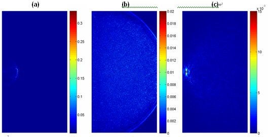
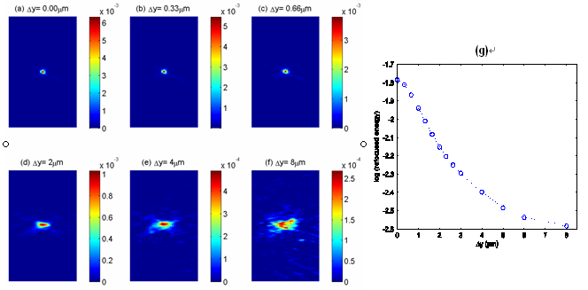
As shown in Fig. 1, PSTD simulation of
light scattering through a macroscopic
cluster of dielectric cylinders and
reflected back by a PCM is shown. After
OPC, light back-traces and refocuses
back to the original location where it
first emerged. Displacement effect (Dy)
of the random media is further analyzed
and shown in Fig. 2. The refocused
light pulse profile for random medium
that is displaced by various
Dy is shown
in (a)-(f). The ratio of the total
refocused energy to the initial total
energy for various
Dy is shown on a
semi-log scale in (g). Notice that as
Dy increases, the refocused light energy
drops rapidly.
The PSTD simulation is a rigorous
simulation technique capable of
simulating light scattering phenomenon
for large-scale problems. Our
simulation results provide important
information to experiments to help
understand the optical characteristics
of OPC.
|
 |
|
Fig. 1. PSTD
Simulation of OPC. |
 |
|
Fig. 2. The
displacement effect of the random medium
on the OPC phenomenon. |
Etching Depth
Dependence of Emission Properties from
InGaN/GaN Light Emitting
Diodes with
Nanohole Arrays: Analysis of Strain
Relaxation and Surface States
Professor Yuh-Renn Wu
Graduate Institute of Photonics and
Optoelectronics, National Taiwan
University
台湾大学光电所 吴育任教授
We apply our simulation models to
analyze the etching depth dependence of
emission characteristic of the InGaN/GaN
quantum well. The effect of strain
relaxation and surface states are
discussed in this work. The device
structures are shown in Fig. 1(a).
Figure 1(b) and 1(c) show the strain
tensors
εxx
with the hole depth equal to
16 nm and 23 nm, respectively.
 |
|
Fig. 1
(a) A schematic of the nanohole
structure. The hole depths are 16nm and
23nm. (b) and (c) show the calculated
strain tensor
εxx
of the nanohole structure with 16nm hole
depth and with 23nm-column hole depth,
respectively. (d) shows the band
structures and wavefunction of 16 nm
nanohole structure at X=73.6nm and
X=10.2nm, respectively. |
As the strain data shown in Fig. 1, the
nanohole structure with 23 nm hole depth
might have a larger blue shift due to
the strain relaxation. In 16 nm hole
depth cases, because of the effect of
surface states at the air/GaN interface,
the fermi level is usually pinned at the
surface states level (~ 0.9eV below
conduction band for GaN). If the cap
layer is thick enough, the effect of the
surface states is negligible. However,
the distance from the surface state to
the quantum well region is only 2 nm in
the cases. The pinning position of the
surface state will strongly affect the
band bending of the cap layer and the
InGaN quantum well layer. When the top
GaN layer is too thin as shown in Fig. 1
(d), the band bending at the GaN layer
is not large enough so that potential at
the left side of InGaN quantum well is
lifted up, which reduces the QCSE
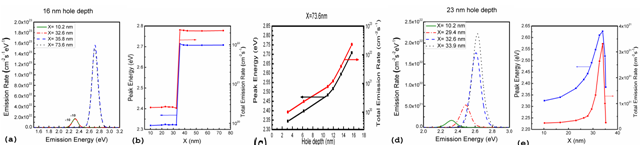
significantly. Figure 2(a) shows the
calculated emission spectrum at
different position of the nanohole. Due
to the surface states pinning effect,
our results show that the emission rate
is enhanced by 82 times and the maximum
of 380 meV blue shift compared to the
unetched region. The etched and unetched
areas have a significant difference in
the emission properties in Fig. 2(b). We
can also find that for the hole depth
larger than 11 nm (~ 7nm to the quantum
well), the emission rates and emission
peak start to have a significant change
in Fig. 2(c). At X = 33.9 nm, the strain
relaxation of quantum well and the
emission rate reaches the maximum as
shown in Fig. 2(d). Fig. 2(e) shows the
emission peak and emission rates versus
different positions X. The emission
property of the nanohole changes
significantly when the hole depth is
close to or penetrates the quantum well.
One is due to the effect of surface
states and the other one is due to the
strain relaxation.
 |
|
Fig. 2
(a) shows the calculated emission
spectrum. The emission spectrum at $X$
=10.2 nm and 32.6nm is multiplied by 10
times to make them clear. (b) shows the
total emission rate and the emission
peak energy versus different positions
for the 16 nm nanohole structure. (c)
The calculated emission strength and
emission peak energy versus different
hole depth. (d) shows the calculated
emission spectrum of the 23 nm nanohole
structure, and (e) shows the emission
peak energy and the total emission rate
versus different positions for the 23 nm
depth nanohole structure. |
In conclusions, we have analyzed the
emission characteristic of InGaN/GaN LED
with depth dependence of the nanohole
structure. The emission property of the
nanohole changes significantly when the
hole depth is close to or penetrates the
quantum well. One is due to the effect
of surface states and the other one is
due to the strain relaxation. Both
effects lead to the blue shift of the
spectrum and the increase of radiation
recombination rates so that it is hard
to be directly determined from
experimental PL measurement. Our
calculation provides useful information
for analyzing the spectrum shift in the
nanohole array and would be very
important factors to be considered when
making these similar structures such as
nanocolumns and nanorods.
Electrical and
Optoelectronic Characterization of a ZnO
Nanowire Contacted by
Focused-Ion-Beam-Deposited Pt
Professor J. H. He
Graduate Institute of Photonics and
Optoelectronics, National Taiwan
University
台湾大学光电所 何志浩教授
We
report on the transport properties of
single ZnO nanowires measured as a
function of the length/square of radius
ratio via transmission line method. The
specific contact resistance of the FIB
Pt contacts to the ZnO nanowires is
determined as low as
1.1x10⁻⁵
Ωcm2. The
resistivity of the ZnO nanowires is
measured to be
2.2x10⁻²
Ωcm. ZnO
nanowire-based UV photodetectors
contacted by the FIB-Pt with the
photoconductive gain as high as ~108
have been fabricated and characterized.
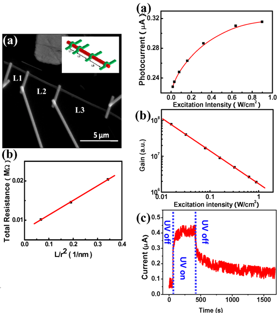 |
|
Figure 1.
(a) SEM image of the test structure of
TLM measurement. (b) Total resistance as
a function of the length over the square
radius of ZnO NW.
Figure 2.
(a) Photocurrent measurement as a
function of excitation power intensity
at applied bias of 0.5 volt. (b)
Photoconductive gain as a function of
excitation power intensity. (c)
Time-dependent photocurrent rise and
decay as obtained by sudden application
(at 60 s) and removal (at 400 s) of UV
light at the bias of 0.5 volt. |
|