發行人:黃升龍所長    編輯委員:蔡睿哲教授    主編:林筱文    發行日期:2008.10.03

最新消息與活動公告    所務公告及活動花絮    邁向頂尖大學計畫研究成果專欄

光電所博士班應屆畢業生研究成果專欄    光電要聞

最新消息與活動公告


   本所10月份演講公告:

日期

講者簡介

講題

地點

時間

10/3 (Fri)

Prof. François Ladouceur

Photonics Group at the University of New South Wales

Photonics Material Research at the University of New South Wales

博理館

101演講廳

14:30-16:30


所務公告及活動花絮


光電所所學會97學年度羽球賽花絮

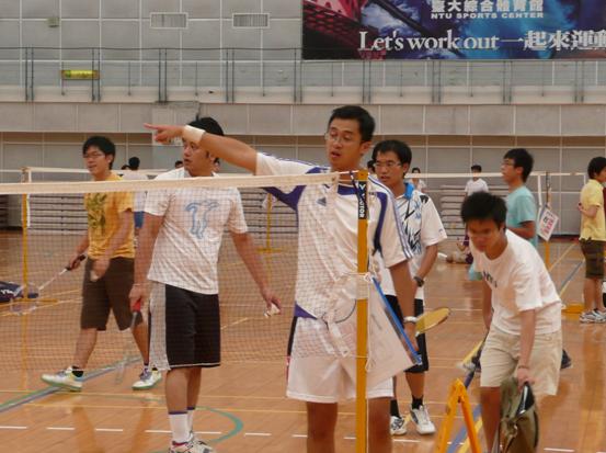
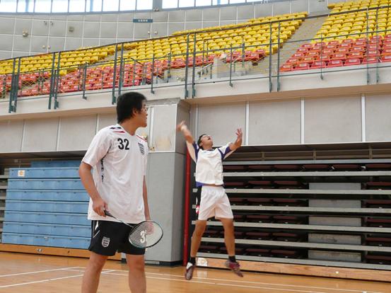
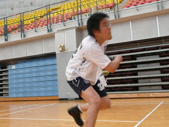
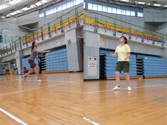
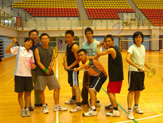
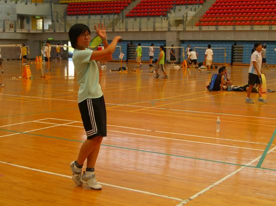
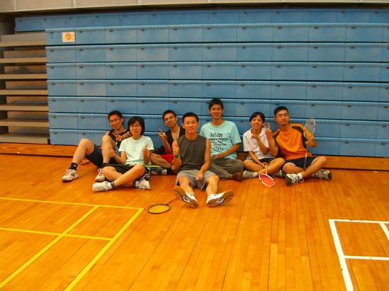
(時間:97年9月8日;地點:台灣大學新體育館3F)

花絮整理:所學會會長劉光中

       今年的光電所羽球大賽,於九月八日下午盛大舉行了。這次參加的隊伍共有8隊,人數達到48人。在經過了三個小時的循環對戰後,由第四隊取得本次大賽的冠軍,另外第二、三、六、七隊積分相同,並列亞軍。比賽之餘還有不少同學雖然沒有來得及報名,但也到場利用場地閒暇之際與大家一同運動, 鼓勵大家多多運動正是本次羽球大賽舉辦的宗旨所在。本次大賽圓滿落幕,在切磋球技、交流感情之際,希望大家也能夠忘懷輸贏,並且再次滿懷著熱情,踴躍參加下一次的光電所體育活動。

參賽同學熱身中 跳殺

肚子也入鏡了

雖然穿著皮鞋依然奮勇作戰

學妹們也參加羽球賽 冠軍隊伍合照

本屆賽事最強選手

場邊休息時合照


邁向頂尖大學計畫研究成果專欄


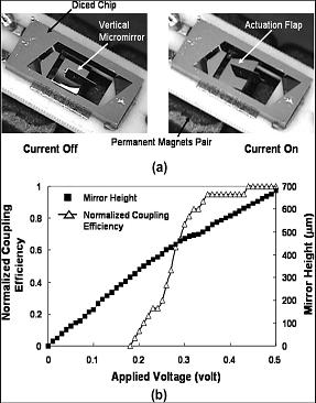
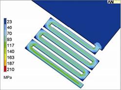
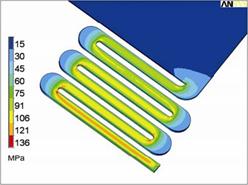
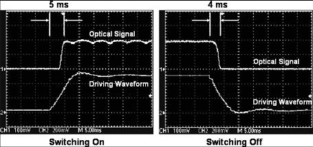
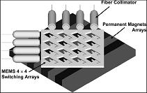
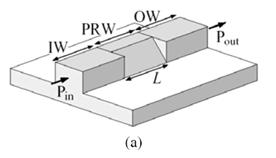
Low-Actuation-Voltage MEMS for 2-D Optical Switches

Hsin-Ta Hsieh and Prof. Guo-Dung John Su

Graduate Institute of Photonics and Optoelectronics, National Taiwan University

臺灣大學光電所蘇國棟教授

 A novel MEMS fabrication process was developed to integrate vertical stress-free micromirrors and electromagnetic actuators without an extra assembly process. The size of the TMAH etched micromirror is 20 μm × 500 μm × 1200 μm, which is large enough to ensure low insertion loss for 2-D optical-switching applications. The surface roughness of the micromirror is measured to be as low as 20 nm by the white light interferometer, which typically results in 0.2-dB optical loss. The center-aligned vertical mirror showed an excellent TDL of 0.05 dB. An appropriate magnetic circuit design reduces the actuation voltage to 0.5 V with a power consumption of about 3.5 mW. A reasonable fast-switching time of 5 ms can be achieved by eliminating the resonant-frequency components of the MEMS switch through edited waveforms. Long-term cycling and mechanical reliability tests proved that the proposed MEMS optical switch can pass the rigorous requirement of optical communications. The PDL and WDL are both less than 0.1 dB.


(a) Operated device and  (b) applied voltage versus normalized coupling efficiency and moving heights.

Stress analysis for corner design effect.

Switching time of a 2-D MEMS switch.

Schematic drawing of a 4 × 4 MEMS optical switch with periodical magnet ribbons.


Finite-Difference Modeling of Dielectric Waveguides with Slanted Facets

Y.-P Chiou, Y.-C. Chiang, C.-H. Lai, C.-H. Du, and H.-C. Chang

Graduate Institute of Photonics and Optoelectronics, National Taiwan University

臺灣大學光電所邱奕鵬教授

  Abstract -- With the help of an improved finite-difference (FD) formulation, we investigate the propagation characteristics of a slant-faceted polarization converter. The formulation is full-vectorial and it takes into consideration discontinuities of fields and their derivatives across the abrupt interfaces. Hence, the limitations in conventional FD formulation are alleviated. Field behaviors across the slanted facet are incorporated in the formulation and hence the staircase approximation in conventional FD formulation is removed to get better modeling of the full-vectorial properties.


 One limitation of conventional finite-difference method is that grids in the computation are normally parallel to the axes in the discretization of field components. Staircase approximation is often required when the fields are cross a slanted interface between two different materials. The convergence is slow due to the staircase approximation as compared to other methods without staircase approximation, e.g. finite-element method. In addition, the full-vectorial properties may not be accurately modeled under such approximation. To get rid of such limitation, our improved finite-difference method is adopted.


 The investigated structure is shown in Fig.1. An x-polarized field is launched from a standard input waveguide (IW). This incident field excites both the first and second hybrid modes of nearly equal modal amplitudes. As these two hybrid modes propagate along the polarization rotating waveguide (PRW), they would become out of phase at the half-beat length and their combined modal fields produce mainly a y-polarized field in the following output waveguide (OW). The polarization rotating waveguideis based on a rib waveguide with one side wall slanted at an angle around 45 degrees.


 In the structure, both hybrid modes have comparable field components in x- and y- directions, and their polarizations are no longer mainly in the x- or y- direction but in the direction parallel or perpendicular to the slanted wall. As shown in Fig.2, the field is periodically converted between x- and y- polarizations. To verify our simulation, finite-element method (FEM) and Yee-mesh-based finite-difference beam propagation method (Yee-FD-BPM) are adopted as shown in Table I. Both electrical and magnetic fields are used at the same time in the formulation of Yee-FD-BPM. Different methods show very good agreement. Furthermore, we also use conventional finite-difference scheme with staircase approximation and index-average approximation to calculate the same problem. We find that the hybrid modes can not be correctly obtained either by our codes or by commercial software. The fundamental modes may become x- or y-dominant modes, not as expected. To sum up, our improved finite-difference scheme can easily handle structures with facets that are not parallel to x- or y-axis, which alleviates the limitation in conventional finite-difference method.


Fig.1 (a) Polarization converter (b) Cross-section view.
 

Fig.2 Power in x- (solid line) and y- (dashed line) polarized fields along the propagation.

 
Table I


Design and Analysis of Compact Slot Waveguide Directional Coupler-Based Polarization Splitter on Silicon-on-Insulator

Professor Ding-wei Huang

Graduate Institute of Photonics and Optoelectronics, National Taiwan University

臺灣大學光電所黃鼎偉教授

 A slot waveguide directional coupler-based polarization splitter on SOI which exhibits excellent polarization splitting behavior for optical signals around 1.55 mm is designed and analyzed. In our design, the silicon photonic wire is covered by air (nc = 1) and patterned on the buried oxide layer (ns = 1.444) of the SOI wafer, where the low-refractive-index region (slot region) is sandwiched by high-refractive-index silicon (nr = 3.474) at 1.55 μm as shown in Fig.1. The schematic layout of the entire device is shown in Fig. 2. The width w and height h of each photonic wire at the slot region is chosen to be 0.21 μm and 0.25 μm; while the width of the slot ws is set to be 0.2 μm due to the limitation of the fabrication capability. The propagation of light in the directional coupler can be expressed in terms of even and odd modes with effective indices ne and no, which are functions of the waveguides spacing g as shown in Fig. 3. By carefully choosing the spacing g (g = 0.48 μm) between the two waveguides, the coupling length of TE mode LTE can be twice that of TM mode LTM, i.e. LTE /LTM = 2. Meanwhile the length of the coupling region of the device is chosen to be L = 2LTM = LTE, thus the two modes can be successfully separated into 2 different output ports. By using FDTD technique, the electric field intensities of the TE- and TM-polarized modes propagating in the device can be calculated as shown in Fig. 4.


Fig. 1 A cross-sectiional view of slot directional coupler-based polarization splitter. Fig. 2 Schematic layout of the entire device.

Fig. 3 Effective indexes of even modes ne and odd modes no induced in TE polarization (neTE, noTE) and TM polarization (neTM, noTM) of a coupler as a function of waveguide spacing g. Fig. 4 Polarization splitting behavior in the device. The left-hand side is the result of TM mode and the right-hand side is the result of TE mode.


光電所博士班應屆畢業生研究成果專欄


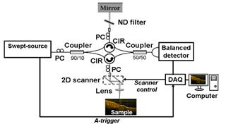
論文題目:光學同調斷層掃瞄技術於口腔癌診斷之研究

姓名:蔡孟燦

指導教授:楊志忠教授

摘要

口腔癌在台灣男性癌症排名第四,對於一般口腔癌病患,早期診斷可高達百分之七十五的五年以上存活率。光學同調斷層掃瞄技術可以提供縱切面的組織造影,並具有高解析、高造影速度以及較深的造影深度 (2~3 mm)等優點,因此光學同調斷層掃瞄技術適合作為口腔癌早期診斷的工具。在這研究中,我們應用光學同調斷層掃瞄技術於離體以及臨床的口腔癌研究。我們建立了一套掃頻式的光學同調斷層掃瞄系統,首先針對從口腔癌病患身上切除的口腔癌樣本做掃瞄。這套系統具備8 μm的縱向解析度以及靈敏度可達108 dB,透過這套系統掃瞄,可區分出正常以及癌組織。

在臨床上,我們將此掃頻式的光學同調斷層掃瞄系統接上一特別設計的掃瞄探頭,在醫院針對口腔癌前病變和口腔癌病患掃瞄,並統計上分析有效的診斷指標。在這部分,我們提出了三種指標,其中包含縱向強度分佈的標準差、由縱向強度分佈的空間頻域頻譜所得到的指數衰減常數(a),以及當上皮層和結締組織間的介面仍存在時,所得到的上皮層厚度。另外,我們分析在統一標準和個別相對標準下,這些診斷指標的靈敏度以及明確度。由結果發現,針對中度上皮變異以及鱗狀細胞癌,標準差以及a值將會是很好的診斷指標。另一方面,上皮層厚度適合用作上皮增生以及中度上皮變異診斷上的指標。另外,我們也利用此可攜式的掃頻式光學同調斷層掃瞄系統來追蹤評估口腔癌病患經由光動力療法治療後其復原情形。我們將列出其中兩位病患治療後的結果,並藉由上述三種診斷指標來分析光學同調斷層掃瞄系統的掃瞄結果。


光電要聞


— 資料提供:影像顯示光電科技特色人才培育中心•影像顯示科技知識平台 —

— 整理:林晃巖教授、陳冠宇 —


IBM開發出採用磁性材料與利用自旋電子學技術之超高密度非揮發性記憶體

 美國IBM與台灣的工業技術研究院(ITRI)宣佈,將合作研發採用磁性材料的非揮發性記憶體“Racetrack Memory”Racetrack MemoryIBM公司阿爾馬登研究中心(Almaden Research Center)的Stuart ParkinIBM院士)所提出的新型超高密度非揮發性記憶體。


 IBMITRI的共同研究小組將探索Racetrack Memory所用的新材料及新構造。ITRI的副院長Ian Chan表示:「透過在多個候選對象中找出最適合Racetrack Memory的材料及構造,可從中得到新的知識。」


 美國IBM發表的新型非揮發性記憶體“Racetrack Memory”是基於自旋電子學(Spintronics)技術,同時具備高存取性能且強固(理論上摔不破)等「半導體記憶體」的優點以及成本低、容量大等「硬碟」的優點。IBM表示,使用Racetrack Memory,可在隨身裝置上儲存50萬首樂曲或3500部電影,這相當於現有隨身硬碟可儲存容量的約100倍。


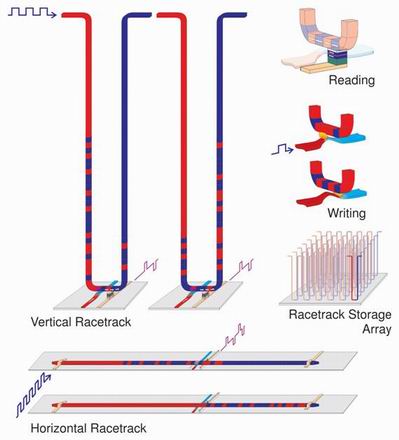
 Racetrack Memory採用記錄在磁性材料中的位列(Bit Column),像賽車跑道那樣排列的構造。因沿垂直或水平於矽底板方向配置的磁性材料可大量記錄資訊,且資料在軌道上跑(the data "races" around the wire "track"),所以不會有移動的讀取裝置,因此更耐用、發熱更低且更省電(一個電池可以讀取一個星期,且不通電時資料可保存十年)。而且既然使用電子的自旋來儲存資料,重複多次的讀取也不會耗損,理論上可以做無限次讀取。


 Racetrack Memory與以往的半導體記憶體相比的優點,是能夠以更小的晶片面積實現大容量。IBM院士Stuart Parkin表示:採用沿矽底板垂直方向配置磁性材料的構造,在理論上可以同時讀取10~100個左右的位元(bits)。即沿垂直方向層疊了約100個由磁性材料形成的位元。這種情況下,磁性材料由物理分割劃分的約100個區域構成,各區域按照磁化方向對資訊“1”“0”進行記錄。


 Racetrack Memory上,向磁性材料的位列施加電流脈衝後,可利用分割記憶體位址的磁壁(magnetic domain walls)發生移動的現象。經過改變脈衝數,可實現對特定位址的隨機訪問。訪問特定位址之後可執行數據的讀寫。此次試製出了包含多個磁壁的磁性材料,並確認能夠利用磁壁移動對訪問對象的記憶體位址進行選擇、讀取、寫入。


圖:Racetrack Memory的結構


參考資料:

“Current Controlled Magnetic Domain-Wall Nanowire Shift Register,” Science, Vol. 320, no. 5873, pp. 209 – 211, 11 April 2008.


原廠發佈資料:

http://www-03.ibm.com/press/us/en/photo/23860.wss

http://www-03.ibm.com/press/us/en/pressrelease/23859.wss


參考中文資料:

http://big5.nikkeibp.co.jp/china/news/semi/semi200804220118.html


版權所有   國立臺灣大學電機資訊學院光電工程學研究所   http://gipo.ntu.edu.tw/

歡迎轉載   但請註明出處   http://gipo.ntu.edu.tw/monthly.htm