 |
||||||||
|
發行人:黃升龍所長 編輯委員:蔡睿哲教授 主編:林筱文 發行日期:2008.09.03 |
||||||||
|
|
||||||||
|
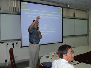
時間:97年8月11日上午10點30分~11點45分
講者:Prof.
Ray T. Chen (Nanophotonics and Optical Interconnects Lab., Department of
Electrical and Computer Engineering, The University of Texas, Austin) Prof. Ray T. Chen於97年8月11日(星期一)蒞臨本所訪問,並於電機二館142會議室發表演說,講題為「Silicon- and Polymer-based Nanophotonic Devices for Optical Communications」,本所教師及學生皆熱烈參與演講活動,獲益良多。
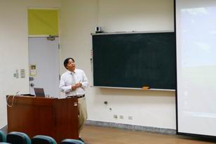
時間:97年8月25日下午3點
講者:何賽靈教授(Joint
Research Center of Photonics of the Royal Institute of Technology
(Sweden) and Zhejiang University (China)) 何賽靈教授於97年8月25日(星期一)蒞臨本所訪問,並於電機二館105演講廳發表演說,講題為「Improving the performances and functionalities of photonics devices with subwavelength-structures and nanoparticles」,本所教師及學生熱烈參與演講活動。
|
||||||||
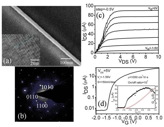
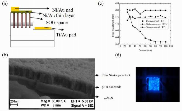
Ferroelectric nitride-oxide nanowire MOSFET and phase change memory Professor Lung-Han Peng's group Graduate Institute of Photonics and Optoelectronics, National Taiwan University (e-mail) peng@cc.ee.ntu.edu.tw 臺灣大學光電所彭隆瀚教授 A. Nitride-oxide nanowire MOSFET
We demonstrated a selective growth of high crystallinity
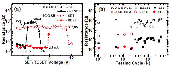
B. Nitride-oxide phase change memory We report a new type of phase-change materials based upon the compound of In-Ga-O. It is found to exhibit two-order of magnitude resistivity change between the high-resistive amorphous phase and the low-resistive cubic phase at a phase-change temperature ~250°C. When the In-Ga-O is incorporated into a nonvolatile phase change memory (PCM) device with a double-heater (DH) structure, it exhibits an on/off resistance ratio of 1000 and cycling over 300 times which are superior to those observed on a single-heater (SH) PCM device. These results, together with a low bias point of 70mA at 6.5 volt and 1.5mA at 3.5 volt, respectively, for set/ reset operation of the DH-PCM device to the crystalline/amorphous state, suggest that In-Ga-O is a promising material candidate for low power application of PCM devices.
|
||||||||
|
論文題目:活體內光學三倍頻分子影像顯微術 姓名:戴世芃 指導教授:孫啟光教授
|
||||||||
|
— 資料提供:影像顯示光電科技特色人才培育中心•影像顯示科技知識平台 — — 整理:林晃巖教授、陳冠宇 —
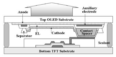
南韓LG顯示器針對OLED面板開發出了稱為“DOD”(Dual-plate OLED Display)的新型面板結構,並於SID 2008口頭報告3.2中發佈。採用這一結構的15吋有機EL面板試製品,也在SID 2008展示會場上展出(如圖一)。
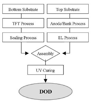
具有DOD結構的有機EL面板由兩塊玻璃底板構成。在一塊玻璃底板上形成薄膜電晶體(TFT),另一塊玻璃底板上形成有機EL元件;並採用了TFT陣列的陽極與有機EL元件的陰極在面板內部接觸的結構(如圖二)。該結構時的製作流程如圖三所示。南韓LG顯示器認為,由於能夠分別單獨地檢查顯示元件,因此與原來在一塊玻璃底板上形成TFT陣列和有機EL元件的有機EL面板相比,能夠防止成品良率下降。
15吋有機EL面板的畫素為1024×768畫素。畫素大小為96μm×297μm,解析度為85.5ppi。畫素開口率為52%。採用從有機EL元件的底板一側獲取光的頂部發光結構。
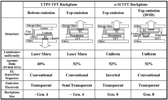
用一個表總結這個技術的優點。低溫多晶矽薄膜電晶體(LTPS TFT)的下發光形式:因為下發光,所以開口率太小;因為低溫多晶矽薄膜電晶體關係無法做大且亮度不均,只能用到第四代基板。低溫多晶矽薄膜電晶體的上發光形式:無法做大;穿透電極為金屬,會有能量損耗,減損出光效率。非晶矽薄膜電晶體(a-Si TFT)的上發光形式:可大至第八代基板,但一路做上來的良率不高。非晶矽薄膜電晶體的DOD形式:基板可做大,發光OLED與控制TFT分開來製作,可以提高良率。
中文新聞出處: http://big5.nikkeibp.co.jp/china/news/news/flat200805230125.html
|
||||||||
|
飯後來瓶清涼飲料超爽!然後…得腸癌 ? 有此一說 最近看到下列文章有點疑惑,請問是真的嗎? 「不要不相信! 很多人習慣吃飽飯後就來一瓶冷飲,尤其是一些罐裝茶飲料,號稱可以「去油解膩」。喝下去是很爽沒有錯,但你有沒有想過接下來你的肚子裡會發生什麼事?! 快動動大腦想想吧!你肚子裡的牛排(或是鹹酥雞、滷味…)都是油膩膩的食物,腸胃要消化本來就比較吃力了。現在再倒入一瓶冰水…有沒有看過冰箱裡面的豬油牛油啊?!你能想像把上面那層白白的凝固油吞進肚子裡嗎?噁!當你的腸胃裡有一塊塊蠟燭般的凝固油,還去什麼油、解什麼膩咧!如果只是噁心的話就算了,重點是—會得腸癌!!這些凝固油碰到胃酸會再度溶解成半液狀,然後會比固態食物早一步流進腸道裡。於是那稠稠黏黏、油不油水不水的物質就會率先被腸道吸收。但是,腸道並沒有辦法完全吸收排除這些詭異的物質,腸璧絨毛會沾滿油脂,就好像冬天要洗牛肉湯的鍋子一樣,怎麼洗都還是覺得油膩膩。而且久而久之這種噁心的東西就會附著在腸道壁上—你總不能往腸子裡倒沙拉脫吧?!經過經年累月的堆積和質變,這些東西輕則導致息肉,更有可能的是病變成腸癌! 所以趕快改掉這種要命的壞習慣!飯後不要馬上灌冷飲,最好是喝點熱湯或溫開水就好啦!然後平常沒事多喝優酪乳。優酪乳可以讓腸道裡多點好菌、趕走壞菌,幫你的腸子來個大掃除,讓腸道更乾淨∼ 」 KingNet
營養保健諮詢營養師回答: 關於上述文章(傳言)的內容,在下認為其「作者」用心良苦,但太過於「危言聳聽」! 飯後立即飲用冷飲的確有礙身體健康。由於人類是恆溫的動物,中心體溫平均為37.5℃,所以過度地食用冰冷的飲品,就很容易造成生理機能減退。例如:腸胃道消化酵素分泌減少,進而造成腸胃消化吸收功能變差,不想吃飯,體重減輕,抵抗力也跟著變弱。這也就是為什麼飯後喝冷飲較被人詬病的原因。
至於,喝冷飲會將豬油、牛油變成固體或半固體的異形物的說法就真的太誇張了!雖說冷飲會影響體溫,但卻只是暫時性的,畢竟人類是恆溫動物,身體有許多生理構造及方法可以立即調整體內溫差,使得生理機能能儘快恢復正常的功能,包括腸胃道裡的酵素機能—脂解酵素(脂肪分解酵素),它是主要分解脂肪的酵素,經由它的幫忙,腸黏膜組織才能順利吸收乳糜微粒。換言之,脂肪在被腸子吸收前,就已經被脂解酵素「處理」過了!並不像上述傳言說的:「腸道並沒有辦法完全吸收排除這些詭異的物質,腸璧絨毛會沾滿油脂。就好像冬天要洗牛肉湯的鍋子一樣,怎麼洗都還是覺得油膩膩。」;其實,別太小看人體生理的構造,但也別太過於「折磨」你的生理器官。一旦身體在被你反覆地「折磨」及「激烈調節」之下,(例如:喜歡冷熱食物交換食用)一旦身體突然地無法負荷,那麼就有可能讓病菌有機可乘,甚至導致任何疾病上身,故不得不小心謹慎。好的飲食習慣,才是最佳的養生之道。 本文由【KingNet 國家網路醫院】提供
|
||||||||
|
版權所有 國立臺灣大學電機資訊學院光電工程學研究所 http://gipo.ntu.edu.tw/ 歡迎轉載 但請註明出處 http://gipo.ntu.edu.tw/monthly.htm |
||||||||