
發行人:黃升龍所長 編輯委員:蔡睿哲教授 主編:林筱文 發行日期:2008.03.03
![]() 賀!本所特聘研究講座蔡振水院士榮獲加州大學爾灣校區(UC
Irvine)校長講座教授(Chancellor
Professorship)之榮譽∼
賀!本所特聘研究講座蔡振水院士榮獲加州大學爾灣校區(UC
Irvine)校長講座教授(Chancellor
Professorship)之榮譽∼
|
本所特聘研究講座蔡振水院士於日前榮獲加州大學爾灣校區(UC Irvine)校長講座教授(Chancellor Professorship)之榮譽,特此恭賀!加州大學系院數年前為了延攬及挽留傑出教授、專家而設立該項講座教授,目前爾灣校區將近兩千位教授中,僅有十八位教授獲聘該項講座。 |
|
![]() 賀!本所林恭如教授獲選為2008
SPIE Fellow∼
賀!本所林恭如教授獲選為2008
SPIE Fellow∼
|
本所副所長林恭如教授於日前獲選為2008年 SPIE Fellow,成為該協會七十二位新成員之一,特此恭賀!SPIE (The International Society for Optical Engineering) 每年遴選光電相關領域研究上具有重要貢獻之學者授予此項榮譽,此次林教授以他於光纖雷射與矽奈米光電元件(fiber lasers and silicon nanophotonics)上之具體成就獲選為2008 SPIE Fellow。相關消息可參見下列網頁:http://spie.org/x32.xml。 |
|
![]() 本所3月份演講公告:
本所3月份演講公告:
|
光電論壇 | ||||
|
3/7 (Fri) |
林瑞騰 博士
New Vision Inc. 董事長,
NCTU(國立交通大學光電工程研究所)
客座教授,
ITRI (工研院/南分院)雷射應用科技中心顧問,
Hon-Hai Technology Group, Consultant.
|
醫療雷射技術之最新進展
Recent Progress in Medical Laser Technologies |
博理館 101演講廳 |
16:30-18:30 |
Advanced Numerical Modelling for Photonic-Crystal and Optical-Waveguide Structures
Professor Hung-Chun Chang
Graduate Institute of Photonics and Optoelectronics, National Taiwan University
臺灣大學光電所張宏鈞教授
A novel analysis method based on a multidomain pseudospectral method is proposed for calculating the band diagrams of two-dimensional photonic crystals and is shown to possess excellent numerical convergence behavior and accuracy. The proposed scheme utilizes the multidomain Chebyshev collocation method. By applying Chebyshev-Lagrange interpolating polynomials to the approximation of spatial derivatives at collocation points, the Helmholtz equation is converted into a matrix eigenvalue equation which is then solved for the eigen frequencies by the shift inverse power method. Suitable multidomain division of the computational domain is performed to deal with general curved interfaces of the permittivity profile and field continuity conditions are carefully imposed across the dielectric interfaces. The proposed method shows uniformly excellent convergence characteristics for both the transverse-electric and transverse-magnetic waves in the analysis of different structures. The analysis of a mini band gap is also shown to demonstrate the extremely high accuracy of the proposed method. (Physical Review E, vol. 75, pp. 026703-1–026703-14, 20 February 2007.)
New full-vectorial optical waveguide eigenmode solvers using pseudospectral frequency-domain (PSFD) formulations for optical waveguides with arbitrary step-index profile are presented. Both Legendre and Chebyshev collocation methods are considered in the formulation. By applying Legendre-Lagrange or Chebyshev-Lagrange interpolating polynomials to the approximation of spatial derivatives at collocation points, the Helmholtz equations for the transverse-electric or transverse-magnetic components are converted into a matrix eigenvalue equation which is then solved for the eigenmodes by the shift inverse power method. Suitable multidomain division of the computational domain is arranged to deal with general curved interfaces of the refractive-index profile together with a curvilinear mapping technique for each subdomain so that field continuity conditions can be carefully imposed across the dielectric interfaces, which is essential in achieving high numerical accuracy. The solver is applied to the optical fiber for the assessment of its numerical performance, to the classical benchmark rib waveguide for comparing with existing high-accuracy results, and to the fused fiber structure for demonstrating its robustness in calculating the form birefingence. (IEEE Journal of Quantum Electronics, vol. 44, no. 1, pp. 56–66, January 2008.)
A finite element method based eigenvalue algorithm is developed for the analysis of band structures of two-dimensional non-diagonal anisotropic photonic crystals under the in-plane wave propagation. The characteristics of band structures for the square and triangular lattices consisting of anisotropic materials are examined in detail and the intrinsic effect of anisotropy on the construction of band structures is investigated. We discover some interesting relationships of band structures for certain directions of the wave vector in the first Brillouin zone and present a theoretical explanation for this phenomenon. The complete band structures can be conveniently constructed by means of this concept. (Optics Express, vol. 15, no. 9, pp. 5416–5430, 30 April 2007.)
A full-vectorial finite element method based eigenvalue algorithm is developed to analyze the band structures of two-dimensional (2D) photonic crystals (PCs) with arbitray 3D anisotropy for in-plane wave propagations, in which the simple transverse-electric (TE) or transverse-magnetic (TM) modes may not be clearly defined. By taking all the field components into consideration simultaneously without decoupling of the wave modes in 2D PCs into TE and TM modes, a full-vectorial matrix eigenvalue equation, with the square of the wavenumber as the eigenvalue, is derived. We examine the convergence behaviors of this algorithm and analyze 2D PCs with arbitrary anisotropy using this algorithm to demonstrate its correctness and usefulness by explaining the numerical results theoretically. (Optics Express, vol. 15, no. 24, pp. 15797–15811, 26 November 2007.)
![]()
![]()
White-light light-emitting device based on surface plasmon-enhanced CdSe/ZnS nano-crystal wavelength conversion on a blue/green two-color light-emitting diode
Professor C. C. Yang’s Group
Graduate Institute of Photonics and Optoelectronics, National Taiwan University
臺灣大學光電所楊志忠教授實驗室
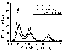
We demonstrate the implementation of a white-light device by spin-coating CdSe/ZnS nano-crystals (NCs) on the top of a blue/green two-color InGaN/GaN quantum-well light-emitting diode for converting blue and green emissions into red light through the absorption/reemission process. Meanwhile, Au nano-particles (NPs) are mixed with CdSe/ZnS NCs for generating localized surface plasmon (LSP) modes to couple with the CdSe/ZnS NCs. The LSP modes can absorb green emission and effectively transfer the energy into the CdSe/ZnS NCs through the coupling process for enhancing red emission. With the LSP coupling process, the conversion efficiency from the blue/green range into red light can be increased by around 30 %. The conversion quantum efficiency can reach 52.8 %.
|
|
 |
|
Fig. 1 Output spectra showing the relative intensities at three injection current levels after the CdSe/ZnS NCs are coated on the blue/green LED. |
Fig. 2 Output spectra showing the relative intensities of the blue/green LED (BG-LED), the CdSe/ZnS NC coating device (NC-coating), and the device of mixed coating of CdSe/ZnS NCs and Au NPs (NC/NP-coating) at the fixed injection current of 15 mA. |
 |
 |
|
Fig. 3 Output spectra showing the relative intensities at three injection current levels in the device of mixed coating of CdSe/ZnS NCs and Au NPs. |
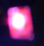
Fig. 4 Picture of the device with mixed coating of CdSe/ZnS NCs and Au NPs. |

寬能隙半導體實驗室---馮哲川教授
本實驗室主要專注在寬能隙半導體材料的應用及分析,其中以碳化矽(SiC)、氧化鋅(ZnO)及氮基半導體為主要研究對象,目前的發展重點如下:
功率與節能應用之塊狀與磊晶碳化矽的創新研究
碳化矽(SiC)在高功率和高溫度元件和節能電子系統中為一種具有吸引力的材料。在高溫,高功率,高頻率和高輻射的先進的節能電子元件中,多晶形態的碳化矽是相當有前瞻性的材料。碳化矽是唯一能被熱氧化形成高品質的二氧化矽的化合物半導體。它能使碳化矽功率電子元件和矽基積體電路科技相結合,開拓新世紀的微電子工程發展。然而碳化矽在台灣的研究發展和工業製造是非常弱的,不像矽基積體電路以及氮化鎵材料和III-V材料的發光二極體的案例那樣,在台灣研究發展和工業製造中占有重要市場佔有率。
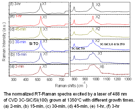
因此本實驗室目前致力發展先進的和創新的磊晶製程,利用先進的高溫低壓化學氣相蒸鍍科技,在大直徑的碳晶片上,來實現立方碳化矽的異質磊晶,並將集中大的努力於研究3C-、6H-、和4H-SiC材料的光學、結構以及表面性質,並探索新的設計,或是改良現有的化學氣相蒸鍍系統。為台灣工業建立良好的基礎去拓展碳化矽高溫化學氣相蒸鍍的研究發展。這將會使台灣在碳化矽的研究發展上,趕上全球的先進水平,並做為學術和工業之間的橋樑,以促進台灣在碳化矽節能電子元件工業的發展。
 |
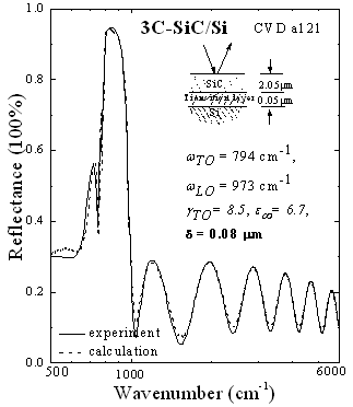 |
| IR reflectance spectrum and theoretical fits, including an interfacial layer, of a CVD-grown 3C-SiC/Si |
矽基薄膜太陽電池界面、表面、缺陷與微結構特性研究
眾所皆知,台灣本身就是一個缺乏能源的國家,所以開闢新能源就是一個十分重要的課題。在人類的生活世界裡,電能消耗是很厲害的,例如,大量電能在各種變電站,電力轉換匣,功能電子元件中被無功地消耗掉。如果我們能發展出新型太陽電池元件,且能工作在惡劣環境下,那將是一即好的解決方法。我們計畫發展新型高效率矽薄膜太陽電池研究以服務於台灣及人類社會。
過去單晶太陽電池佔據市場的主要份額。目前矽薄膜太陽電池已逐漸成為太陽能市場的主流技術,主要原因為薄膜太陽電池比起單晶太陽電池具有生產成本較低及可大量減少矽材料使用量等優點。
本實驗室將致力於矽基薄膜太陽電池界面、表面、缺陷與微結構特性研究,並且提供各階段太陽電池及薄膜生長的快速檢測與深入的科學技術研究,以期了解掌握並克服製作高效率薄膜太陽電池的技術障礙。
|
氮化鎵基(GaN-based)材料及藍光二極體 著重於研究金屬氧化物化學氣相磊晶(MOCVD)技術相關的發光暨缺陷工程,研究生長過程的缺陷和問題,深入發光機制的物理內涵,探索新路徑以控制生長過程的缺陷且利用來增進發光的特性,以製成高質量的氮化物磊晶材料,利用多種的技術作跨領域的研究為研究計畫所強調的重點。
|
 |
 |
 |
 |
 |
|
氧化鋅(ZnO)及相關材料 ZnO、 = 3 \* ROMAN III- = 5 \* ROMAN V和InAlGaP等材料也在本實驗室研究計畫內,其中ZnO被認為是發光材料及元件產業中下世代的熱門材料,而InAlGaP和AlGaAs材料則在半導體發光二極體和雷射產品中應用頗廣,特別是在紅光至近紅外光波長範圍的發光二極體,這些紅光二極體結合氮化鎵為基礎的藍光二極體,可形成白光發 光二極體的全頻光譜,因此,研究計畫也包含一部分為MOCVD磊晶成長InAlGaP和AlGaAs的異質結構。
|
 |
 |
 |
— 資料提供:影像顯示光電科技特色人才培育中心•影像顯示科技知識平台 —
— 整理:林晃巖教授、陳冠宇 —
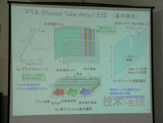
![]() 新興顯示器PTA企圖攻佔超大尺寸、超薄型顯示器市場
新興顯示器PTA企圖攻佔超大尺寸、超薄型顯示器市場
雖然2008年初消費性電子展電漿顯示器陣營紛紛推出超薄型電漿電視,然而電漿顯示器陣營所展示機種的厚度仍然不若LCD或OLED面板/TV般那麼薄。以目前電漿顯示器所用玻璃基板厚度2.8 mm來計算,因電漿顯示器同時需使用2片玻璃基板,故僅是玻璃基板厚度即達到5.6 mm,此外尚需計算2片電漿顯示器前、後基板中間阻隔壁的厚度0.15 mm。
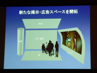
然而目前有一種與電漿顯示器發光原理相似的PTA顯示器,其整體面板厚度可達到僅1 mm。PTA的全名為Plasma Tube Array, 從字面上的意思可了解到其發光原理與電漿顯示器相同,但又為「管狀」陣列的顯示器。電漿管陣列(PTA)顯示器的基本結構,在直徑1mm真空玻璃管內,依序製作放電保護膜、螢光體、放電氣體,形成與電漿顯示器完全相同的發光結構。上述真空玻璃管稱為電漿管(Plasma Tube),電漿管依照R、G、B複數排列,正面與底部分別粘貼設有電極的透明外部電極基板,因此,PTA面板有如眾多併列的玻璃細管,再加上Film狀的電極覆蓋上去所組成。電漿管是利用包覆玻璃管壁形成的放電空間,利用顯示電極與位址電極施加電壓,形成與AC型電漿顯示器的3電極放電結構完全相同的電極構造。除了使用傳統電漿顯示器的灰階驅動技術,亦即ADS(Address Display-period Separation)次場界(sub field)技術之外,同時還直接沿用電漿顯示器的驅動電路基本結構與電極驅動IC等關鍵性周邊元件。直徑1mm的真空玻璃管以R、G、B一組為單位構成間距3 mm的畫素,接著在水平方向並排設置1000~2000個畫素(總長度大約是3~6 m),就能夠獲得相當於對角尺寸150~250英吋超大型畫面。
 |
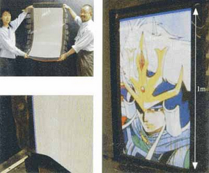 |
PTA顯示器主要開發廠商為「篠田Plasma株式會社」, 該會社是取名自該會社代表取締役會長、有電漿之父稱號「篠田傳」的姓。篠田傳於1973年任職於富士通株式會社,自此以後皆從事電漿顯示器研究開發工作,其於電漿顯示器成就包括於1983年發明彩色電漿顯示器的基本構造,1992年開發世界第1台21吋全彩電漿顯示器等。篠田傳於2005年6月成立篠田Plasma株式會社,專門研發與製造PTA顯示器,PTA試製品第1次在2007年日本尖端資訊與電子展 (Cutting-Edge IT & Electronics Comprehensive Show) 公開亮相,該顯示器為43吋、重量僅800公克。2008年1月底,篠田Plasma株式會社一改過去單打獨鬥的態勢,開始與「株式會社ULVAC」、「藤森工業株式會社」、「大電株式會社」策略聯盟。篠田Plasma株式會社除與上述3家廠商在PTA顯示器領域進行生產與技術上的合作外,並獲得資金方面的挹注。「株式會社ULVAC」為負責開發PTA顯示器相關的生產設備,而該公司並出資1億日圓(約93.6萬日圓)予篠田Plasma株式會社;在此之前,株式會社ULVAC主要是平面顯示器的設備裝置製造公司。「藤森工業株式會社」則負責film狀電極的開發,並出資5,000萬日圓(約46.8萬日圓),該公司同時製造可降低光線反射的電漿顯示器用濾光片(filter)。「大電株式會社」主要為從事螢光體材料的開發,螢光體材料幾乎與電漿顯示器完全相同,其出資金額為4,000萬日圓(約37.5萬美元)。
PTA的優點在於PTA面板厚度不到電漿顯示器的1/5、重量亦為一般電漿顯示器 的1/10、耗電量僅為同尺寸電漿顯示器的1/2、且不需大型生產設備及無塵室設施等;相對而言,LCD與電漿顯示器隨玻璃基板大型化,投資金額呈等比級數增加。雖然PTA 顯示器容易可達到100吋以上的大螢幕,然而現階段最明顯的缺點為解析度不夠精細,2個畫素之間的間距即高達3 mm,故初期與LED顯示器同,將先行導入公用顯示器市場,又PTA顯示器具超薄、輕量、低耗電量、可撓等特性,故能放置於屋頂天花板上、嵌入地板內、貼附在彎曲狀的牆壁或圓柱狀物體上、及製作成超寬型螢幕(例如賽馬場、足球場用途)等。
 |
篠田Plasma株式會社預計於2008年上半開始量產PTA面板,計劃於2008年下半出貨予系統廠,最快將於2009年將開始銷售,並將以150吋為優先導入尺寸,預定屆時上市價格能與同尺寸LED顯示器匹敵。
新聞出處:
http://www.digitimes.com.tw/n/article.asp?id=0000081458_A7H2SD3XDT6LN5S7W86SW
http://tech.digitimes.com.tw/print.aspx?zNotesDocId=0000050718_B6JLFZ8FRX0EUT29ADUJI
http://big5.nikkeibp.co.jp/china/news/flat/flat200711010116.html
偶爾禁食,可以讓身體器官適度休息?
![]()
有此一說:
請問以下內容是真是假?
您好,我聽我同事說,因為現在的人生活太富裕,吃太多魚肉等食物,讓肝腎有過多的負荷,所以有時候一天不吃東西只喝水或優酪乳,可以讓它們能適度的休息,不曉得這是不是正確的觀念?謝謝!
KingNet
營養保健諮詢科營養師回答:
(桃園敏盛綜合醫院健康美學中心 陳正育營養師)
禁食或者是斷食法,其實不完全是挨餓,所謂禁食,即是減少我們平時進食的份量,再以果菜汁代替,以補充能量,而這樣的方法已經沿用了好幾世紀,無論中外都曾用過這種方法來調養生息,但是禁食應該經由專業的醫事人員指導下進行,不可自行貿然採用,根據國外的研究顯示,熱量(飲食卡洛里)的限制,可能能夠延長人類的壽命,尤其是對於中老年人,換言之,吃得越多並不代表大富大貴,相反地吃太多將可能是萬病的根源,最近有文章發表在猴子身上這種理論已經獲得證實。
更激進的,有人甚至主張這種總熱量攝取的降低對於某些癌症可能會有限制癌細胞生長的效果,而這種理論最近在著名的癌症研究期刊中發表 (
Journal of the National Cancer Institute 1999;91:489-491,512-523),引起學界的注意。
研究者是哈佛大學醫學院的Dr. Purna Mukherjee,
它們以兔子為對象,將攝護腺癌細胞植入各種不同熱量攝食組的實驗兔體內,
發現癌細胞的重量在限制熱量20%的一組,竟然降低了62%,而限制熱量40%的一組,則降低高達76%;總之,適時地減少熱量的攝取,乃至於短時間的斷食,的確能給身體器官有個喘息的機會,進而提高身體的機能。
只不過方法一定要正確,除了需要經醫師的指導之下進行外,禁食期間勿僅僅喝水而已,還須配合補充膳食纖維(例如果菜汁、燕麥麩、甚至是蘆薈汁),但切記!患有糖尿病者不可以嘗試禁食法!
本文由【KingNet 國家網路醫院】提供
版權所有 國立臺灣大學電機資訊學院光電工程學研究所 http://gipo.ntu.edu.tw/
歡迎轉載 但請註明出處 http://gipo.ntu.edu.tw/monthly.htm